Al:ZnO thin films were deposited using the radio frequency magnetron sputtering technique at various temperatures and sputtering powers. With the increase in the deposition temperature and the decrease in the radio frequency sputtering power, the crystallinity was increased and the surface roughness was decreased, which lead to the decrease in the electrical resistivity of the film. It is also clearly observed that, the intensity of the (002) XRD peak increases with increasing the substrate temperature
The transparent conducting oxide means the excellent film of optical transmittance[3] about visible rays area of high electrical conduction mechanism and 400~800 nm wavelength. Currently the most frequently used Transparent Conductive Oxide(TCO) is Indium Tin Oxide(ITO). ITO has transmittance(≥90%), low specific resistance(≤10-3 Ω/cm) in the visible rays area, so it is used as the transparent electrode of the solar cell, display fields widely. But the raw materials of ITO are expensive [4], and it has weak point of the degradation phenomenon and toxicity when it is exposed in the hydrogen plasma. In order to address the shortcomings of these ITO, a study on adding the various impurities to ZnO and SnO2 was conducted [5]. The doped ZnO is researched about impurities such as Al, Ga, In, B etc. by the transparent electrode type.
The Al of doped ZnO(AZO) thin film is cheap and controlling of specific resistance is easy, and the wavelength of the visible rays shows the high transmittance, so a lot of studies on the transparent conducting oxide are being conducted.
In this study analyzed and produced AZO thin film for transparent conducting oxide application of the solar cell by the RF magnetron sputtering method [6,7].
This experiment AZO thin film by using Radio Frequency(RF) (13.56 MHz) magnetron sputtering equipment(×10-8 torr), and ZnO(98 wt/%):Al2O3(2 wt%)[8], thickness 1/4“THKΦ2"ceramic
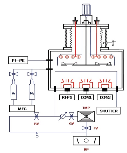
target was used and the distance between the target and substrate was fixed with 4cm. The device which was used for AZO thin film was high frequency magnetron sputtering device(KVS-660, Korea Vacuum), and the instrument diagram is as Fig. 1.
The substrate temperature was around at room temperature, the initial vacuum for sputtering was 3.0×10⁻⁶ torr, and the pressure was controlled by injecting Ar gas using a Mass Flow Controller(MFC) after exhausting. As working gas, the purity 99.999% argon gas was used[9], and the working pressure was fixed with 1×10⁻² torr. RF power was metalized by converting in 150~225 W. About 400~600 nm AZO thin film was formed by sputtering at different power setting for 5~20 min.
3.1 Structural characteristics of AZO thin film depending on AZO thin film
Figure 2 shows Atomic Force Microscopy(AFM) surface measurement of results of deposition thin film on the soda lime glass(SLG) substrate when the sputter power was changed. As the power is increased, he uniform particles with increased size was formed gradually. It can be seen that these results match the size of the grid calculated with XRD measurements values. The reason of growth of crystallizing as the power is increased depending on the picture of AFM surface, is that high more zinc ion with high volatility is sputtered in the target about plasma energy than oxygen ions as the power is increased, so it is metalized in the substrate.
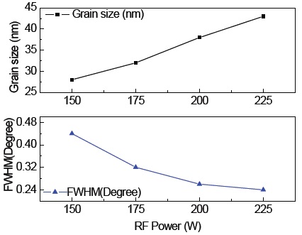
Figure 3 shows FWHM of grain boundary size depending on RF power. As Fig., the FWHM value decreased from 0.44 into 0.24 as RF power is increased. and grain size increased from 28 nm into 43 nm as RF power is increased.
It can be seen that the size of grain boundary became bigger from that FWHM decreased.
3.2 Characteristics of thin film depending on the post-weld heat treatment changes in temperature
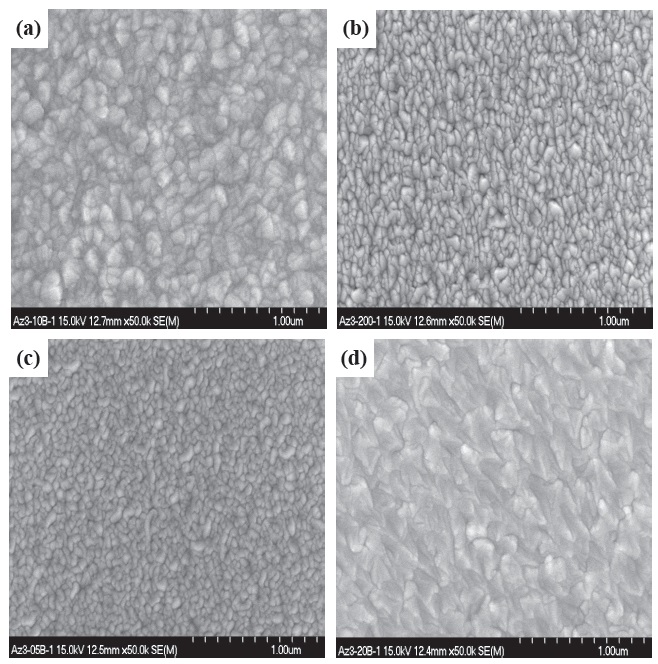
Figure 4 SEM image shows the surface pictures of crystallizing depending on the heat treatment changes in temperature of AZO thin film. As the heat treatment temperature increased, the grains generated in the crystallizing surface are formed relatively
small and uniformly gradually. These results are similar with SEM results related to crystallization depending on the evaporating temperature of substrate which was conducted above.
It could be seen that the elliptical uniform particles were generated
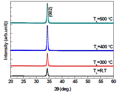
on the general surfaces in 400℃, thus the crystallization was improved. This is similar with XRD results Fig. 5. The heat treated thin film increased in 500℃ more than interval between particles is 400℃. In addition, through experiments, the thin film evaporation produced at room temperature improved crystallization by providing lacked crystallization energy in the postweld heat treatment process during sputtering.
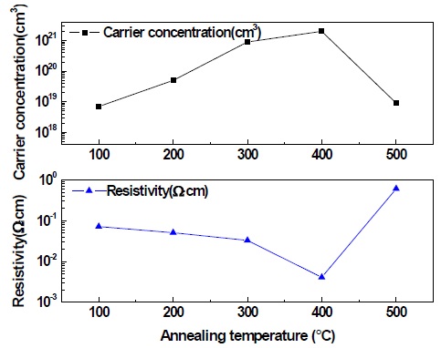
Figure 6 shows specific resistance characteristics depending on the heat treatment changes in temperature. Looking at the specific resistance results of heat treated thin film from thin film which was metalized at room temperature, as the heat treatment process temperature increased up to 400℃, the specific resistance characteristics was improved. By providing necessary energy for crystallization through heat treatment process, the atoms were expanded enough in the particles, and as the thin film formed the uniform and stable surface, the electron concentration of the particles surface increased. But when the heat treatment temperature increased with more than 400℃, the rapidly specific resistance value decreased. At a heat treatment, of over 400℃, cracks occurred during in crystallizing due to the difference between the coefficient of thermal expansion of the substrate and coefficient of thermal expansion of thin film, so the leakage current increased, and the characteristics of thin film is judged that decreased due to the composition of each structure and the decrease of free electron.
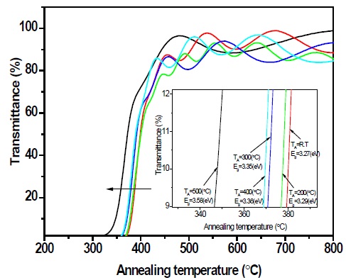
Figure 7 shows optical transmittance of AZO thin film depending on the heat treatment changes in temperature for evaporation of thin film. The substrate shows average 85% of optical transmittance from 380 nm to 800 nm as absorption edge. The thin film produced in more than 300℃ achieved more than 80% of optical transmittance in the visible rays area. As the heat treatment temperature increased, the optical transmittance moved to
the ultraviolet rays area as the blue shift.
This study aims to produce AZO thin film for transparent conducting oxide application of solar cell by RF magnetron sputtering method, and to derive optimal conditions so to improve the ensuring reproducibility and characteristics about properties of AZO thin film, and to develop the high efficiency solar cell through the property characteristics of thin film depending on the rapid heat treatment temperature.
1. The reason of growth of crystallizing as the sputter power increased, is judged that more zinc ion with high volatility is sputtered in the target about plasma energy than oxygen ions as the power is increased, so it is metalized in the substrate, and the size of grain boundary became increase with a decrease of FWHM. The grain boundary increased from 28 nm to 43 nm as the RF power increased. As the grain boundary increased, the scattering phenomenon decrease can expect the improvement of degree of mobility of AZO thin film.
2. As heat treatment temperature of AZO thin film increased, the grains generated in the surface of crystallizing is formed relatively small and uniformly. The heat treated thin film increased in 500℃ more than interval between particles is 400℃. In addition, through experiments, the thin film evaporation produced at room temperature improved crystallinity by providing less crystallization energy in the post-weld heat treatment process during sputtering.
By providing necessary energy for crystallization through heat treatment process, the atoms were expanded enough in the particles, and as the thin film formed the uniform and stable surface, the electron concentration of the particle surfaces increased.
The optical transmittance shows average 85% of optical transmittance of AZO thin film depending on the heat treatment changes in temperature from 380 nm to 800 nm as absorption edge. The thin film produced in more than 300℃ achieved more than 80% of optical transmittance in the visible rays area. As the heat treatment temperature increased, the optical transmittance moved to the ultraviolet rays area as the blue shift.