Transparent conducting oxide films are used by applications in microelectronic systems, such as flat panel display and thin film solar cells [1,2]. Among the known TCO materials, indium tin oxide (ITO) material has been used extensively, as it yields excellent electrical properties. However, ITO thin films have disadvantages, such as toxicity, high price and instability in hydrogen plasma. Zinc oxide (ZnO) is a wide optical band gap material with a wurtzite hexagonal structure, which exhibits a change in conductivity when doped with Al, Ga, and In [3]. However, the resistivity of these thin films is high and mechanical flexural properties are low. In order to improve the electrical and optical properties of transparent conducting films, the multilayer films consisting of a metal layer and semiconductor layers have been studied, such as ZnS/Ag/ZnS [4] ITO/Ag/ITO [5], and ZnO/Ag/ZnO [6]. For ITO/Ag/ITO multilayer films, ITO lacks the high refraction that requires reducing the strong reflection from the Ag layer [4]. Due to the high refraction of ZnO, ZnO/Ag/ZnO multilayer films with high transmittance and conductivity have been studied [6]. In this paper, multilayer (AZO/Ag/AZO) films were prepared on polyethersulfon (PES) substrate at room temperature by using the Facing targets sputtering method. Moreover, the multilayers exhibit stable mechanical properties compared to the single-layered TCO sample during the bending test due to the existence of the ductile metal layer.
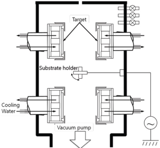
Figure 1 shows the diagram of the facing targets sputtering (FTS) system used in the multilayer thin film deposition process. The FTS system was designed to array the two targets to face each other and so form high density plasma between the targets. The FTS system was able to restrain the bombardment of the substrate by high-energy particles because the position of the substrate was located outside of the plasma. Consequently, the FTS system suppresses the substrate damage caused by high-energy particles, such as electrons and partial ions [7-10]. In this work, Ag targets were installed on top
and the AZO targets were installed on the bottom. The chamber was evacuated to 2.6 × 10⁻⁴ Pa before the film deposition began using a rotary pump and a turbo molecular pump. Before each run, the target was pre-sputtered in a pure argon atmosphere for 10 min in order to remove the natural surface oxide layer of the Ag and AZO targets. The PES substrate was ultrasonically cleaned using isopropyl alcohol (IPA) and DI-water at 30 min and was blown dry with N2 gas. More details about the sputtering conditions are given in Table 1. The thicknesses of multilayer thin films were measured by using a surface profiler (alpha-step). Electrical properties of the films were measured by using a four-point probe. Optical transmittance and structural properties were measured by using UV/VIS spectrometer, X-ray diffractometer, and field emission scanning electron microscopy (FE-SEM). Finally, mechanical flexural strength of the single-layered AZO and the multilayer were measured by using a bending tester.
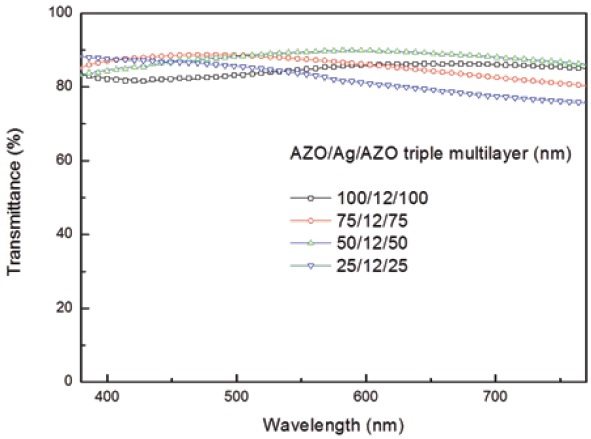
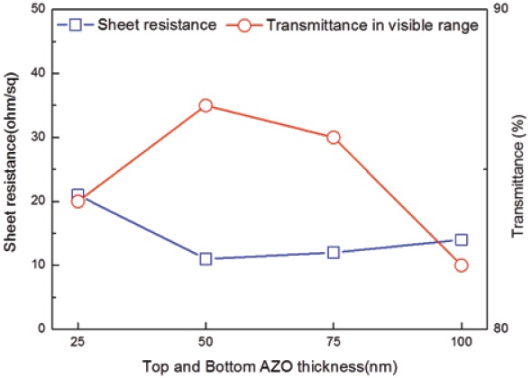
Electrical and optical properties of the multilayer should be excellent. Therefore, we measured sheet resistance and optical transmittance in visible range (380-770 nm wavelength). Figure 2 shows the optical transmittance of the AZO/Ag/AZO multilayer in visible range
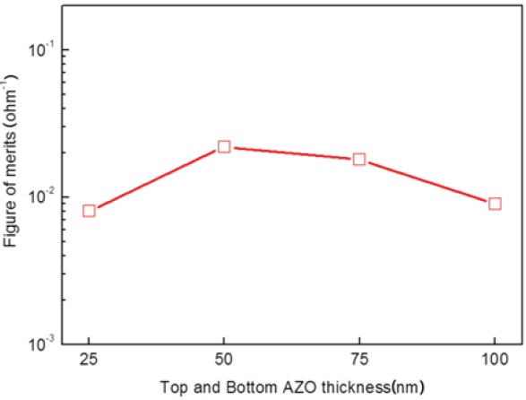
as a function of AZO thicknesses. The maximum average transmittance is 87% with the AZO thickness of 50 nm. The AZO layers play the role of anti-reflective coatings in the multilayer films. This result is consistent with that reported by Leftheriotis et al [11]. As the AZO thickness increases further to 100 nm, the average transmittance decreases. Figure 3 shows the sheet resistance and average optical transmittance in visible range of the multilayer as a function of AZO thicknesses. The sheet resistance of multilayer films shows 21, 11, 12 and 14 Ω/□ with 25, 50, 75 and 100 nm AZO thicknesses, respectively. The average optical transmittance of multilayer films in visible range shows 84, 87, 86, and 82 with 25, 50, 75 and 100 nm top and bottom AZO thicknesses, respectively. Figure 4 shows the figure of merits (=FOM) suggested by Haacke [12] as a function of the AZO thicknesses. In various applications of transparent conductive films, the optical and electrical properties of the films are very important. Haacke [12] proposed a figure of merit followed by:
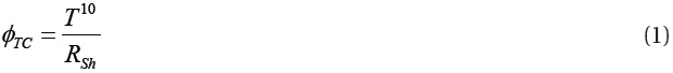
Where T is the average optical transmittance and Rsh is the electrical sheet resistance of the TCOs. This equation can be used to compare the performance of transparent conductive films. The maximum value (= 2.2 × 10⁻² Ω-1) is found when the AZO thickness was 50 nm (T: 0.87 and Rsh: 11 Ω/□).
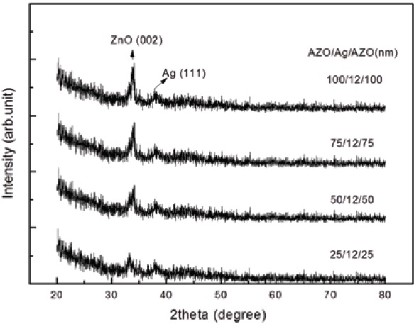
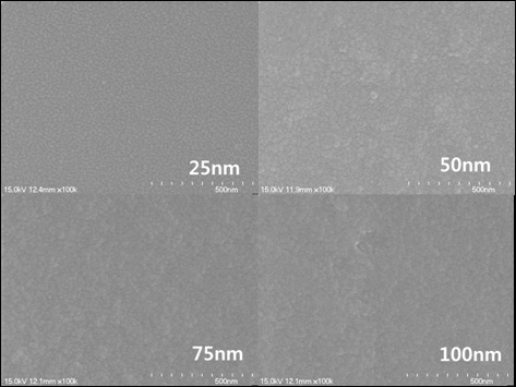
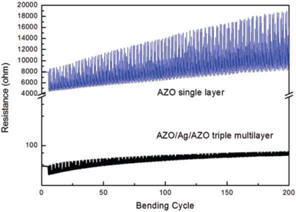
Figure 5 shows the XRD patterns of multilayer films as a function of AZO thicknesses. For all samples, the ZnO(002) and Ag(111)peaks are observed, and the intensity of the (111) peak is much weaker than the (002) peak. As the AZO thickness increases from 25 to 100 nm, the intensity of the (002) peak increases and the intensity of the (111) peak increases slowly, which suggests that the crystallinity of the AZO and Ag layer is simultaneously improved. The AZO thickness dependence of crystal size for the AZO/Ag/AZO multilayer films is investigated by FE-SEM analysis. Figure 6 shows the micrographs of AZO/Ag/AZO multilayer films as a function of AZO thicknesses. When the AZO thickness increases from 25 to 100 nm, an increase in the size of crystallite is observed. Figure 7 demonstrates the mechanical flexural strength of single-layered AZO and multilayer films. The resistance of single-layered AZO thin film rapidly increased above 100 cycle. However, the resistance of the multilayer was constant. Moreover, the multilayers showed more stable mechanical properties in comparison to the single-layered AZO sample during the bending test due to the existence of the ductile Ag metal layer.
Electrical, structural, and optical properties of the AZO/Ag/AZO multilayer structure on polyethersulfone substrate were investigated
as a function of top and bottom AZO thicknesses. From the results, the sheet resistance and average optical transmittance of AZO/Ag/ AZO films with a thickness of 50/12/50 nm are 11 Ω/□ and 87%, and the figure of merit exhibits 2.2 × 10⁻² Ω-1. Moreover, the multilayers demonstrated more stable mechanical properties compared to the single layered AZO sample during the bending test due to the existence of the ductile Ag metal layer. Thus, AZO/Ag/AZO multilayer thin films could apply flexible transparent electrodes.


![The figure of merits (=FOM) suggested by Haacke[12] as a function of the AZO thicknesses.](http://oak.go.kr/repository/journal/11941/E1TEAO_2013_v14n1_9_f004.jpg)