In recent years, rechargeable battery composed of lithium-ion or lithium-ion polymer has been widely used in mobile phones and notebook computers. Since the beginning of the commercial production of the battery, it becomes a device with a higherenergy and smaller volume. The safety circuit of a rechargeable battery is important for a harmless and high-efficient energy solution. The safety circuit usually requires a power metal-oxide-semiconductor field-effect-transistor (MOSFET) in the switching regulation of the protection integrated circuit (IC) [1].
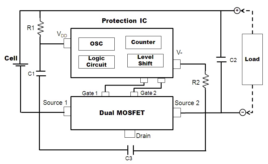
The dual MOSFET switch is applied in protection IC as shown in Fig. 1. The structure of the protection circuit module (PCM) for a rechargeable battery is composed of a protection IC, dual power MOSFETs, and passive components. The charging and discharging characteristics of a rechargeable battery are measured through gates 1 and 2 of the power MOSFET. The protection IC is composed of a counter, oscillator, logic circuit, and level shifter. The logic circuit and level shifter control the gates. The protection IC and dual MOSFET are fully integrated with off-chip resistors and capacitors in order to obtain high speed and low power PCM. The operation of the battery protection IC includes protection against over-charge, over-discharge, and over-current, which may cause overheating and disable the battery. When the protection IC detects an abnormal operation, the MOSFET switch is switched off and waits until the normal operation returns. In this system, the n-channel dual MOSFET performs an essential role by switching on the gate 1 or gate 2, and this eventually charges or discharges the battery load. Obviously, it is desirable to assemble the load-switching power MOSFET into a low profile package for any electric applications.
Compared to a bipolar power transistor, the power MOSFET [2-6] is a voltage controlled device with high input impedance. Its small input current and high switching speed enables it to increase its application in low power high frequency switches. In addition, power MOSFET has a low gate current during switching between the on and off states:, relatively large drain currents can therefore be switched with negligible gate current. However, power MOSFET has problems of electrostatic discharge and is difficult to protect under short circuited fault conditions. Without a safety margin or proper regulator, the power MOSFET breaks down and the protection IC can become useless. The basic operation of power MOSFET is almost the same as that of any MOSFET. The drain-to-source blocking voltage is usually in the kilo-volt range and the current handling capability may be in the range of 0.05 to 1 ampere.
The two basic power MOSFET structures are DMOS and VMOS devices. The VMOS power device is a nonplanar structure that requires a complicate fabrication process. A V-shaped groove is formed for the channel, extending through to the drift region. On the other hand, the DMOS device uses a double diffusion process. The surface channel length is the difference in the lateral diffusion distance between the base and the source. The parasitic n+pnn+ (p+npp+) vertical bipolar transistor structure in the DMOS device can increase the breakdown voltage. In this work, VDMOS structure is applied, which implies that both surface and vertical channels improve the channel current.
In an electronics application, the power MOSFET switch must be protected even at a high electro-static-discharge (ESD) voltage or a reversed battery connection. For example, in power integrated circuits with a built-in control circuit, a parasitic diode is usually formed between the ground and the supply voltage terminals. Under a reversed battery connection, an excess current can flow through the parasitic diode and destroy the power integrated circuits. To protect the power IC and rechargeable battery, a power MOSFET is usually added in series with the control circuit.
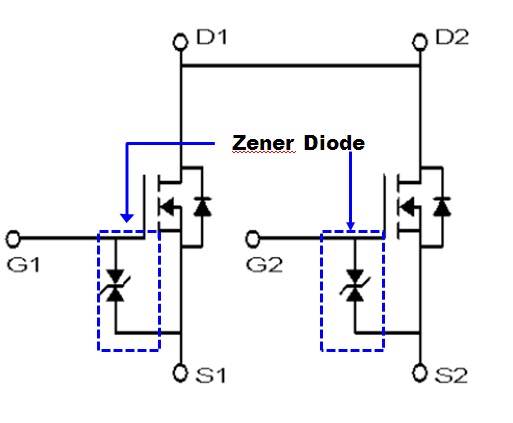
This paper describes a dual power MOSFET switch, which is controlled by the protection IC. In order to protect the gate oxide in the MOSFET and bypass any high ESD voltage, a Zener diode [7] is connected between the gate and source of the dual power MOSFET switch. The aim of the application is to bypass any high peak voltage during the transient time and to provide a weak clamped voltage. In this work, the Zener diode is located on the top of the gate oxide of the power MOSFET. Electrical characteristics of the power MOSFET are measured with the variation of the doping concentration in the Zener diode.
The dual MOSFET switch is shown in Fig. 2, and which is composed of two power MOSFETs, Zener diodes, and diodes. The application voltage of the power MOSFET is typically within the hundreds or kilo volt range. In this application, MOSFET traverses the current-voltage characteristics from the cutoff through the active region to the ohmic region as the device turns on and off. When MOSFET is driven by a large gate voltage and in the switching ON state, it is driven into the ohmic region. Such a high voltage can cause the gate oxide to breakdown. The purpose of the Zener diode is used to improve the endurance voltage of ESD and to maintain a constant voltage across the gate oxide, even when the gate voltage changes. Good regulation requires that the breakdown voltage be maintained above some minimum current with low power dissipation. The breakdown voltage of the Zener diode is relatively constant over a wide current range.
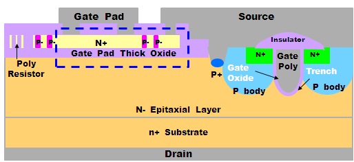
A cross section of the power MOSFET with the Zener diode is shown in Fig. 3, where the MOSFET is composed of a drain, an nepi (drift region), a gate, and a source. The source is composed of a p body and N+ region.
The gate includes a gate poly and a gate pad. Zener diode is situated between the gate pad and the thick oxide. The parameters in n-epitaxial layer have restrictions in the breakdown voltage and on-state resistance, while the switching and frequency performance mostly depend on the parameters in channel region. With the output node constrained to swing from ground to VDD, the drain-to-body junctions in the n-channel device are always reversed-biased.
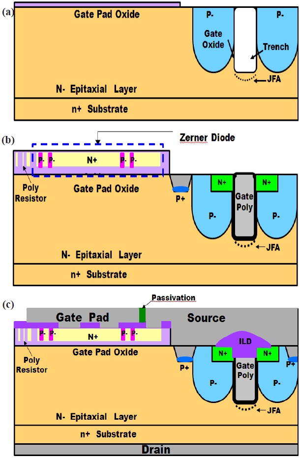
The process sequence is shown in Fig. 4. The n- silicon epitaxial layer with thickness of 3 μm is grown on top of the n+ high doping substrate. A gate oxide is grown with thickness of 300 Å and the p-diffusion is then diffused for the p-body (step a). A thick layer of poly silicon is deposited for the gate poly and the Zener diode. Boron and phosphorus are diffused with the doping concentrations of 1 × 10¹⁵ and 5 × 1015 cm-3 for the p-/n+ Zener diode (step b). Step c shows metal deposition and passivation.
Metallization for gate and source pads occurs by the nickel-aluminum composite.
The breakdown voltage of the Zener diode is measured with a variation of the p-(boron) doping concentration in the Zener diode. The heart of the power MOSFET switch consists of the gate oxide and the Zener diode. As shown in Fig. 4, the Zener diode is located on the top of the gate pad oxide. The doping concentration in diode can affect the carrier distribution and charge trap in the channel. The energy bands in the semiconductor adjacent to the gate oxide interface bend depending on the applied voltage and the doping concentration of the channel. The threshold voltage is the applied gate voltage required to achieve the threshold inversion point. The space charge density at the threshold inversion point can be affected by the acceptor doping concentration and the charge trap.
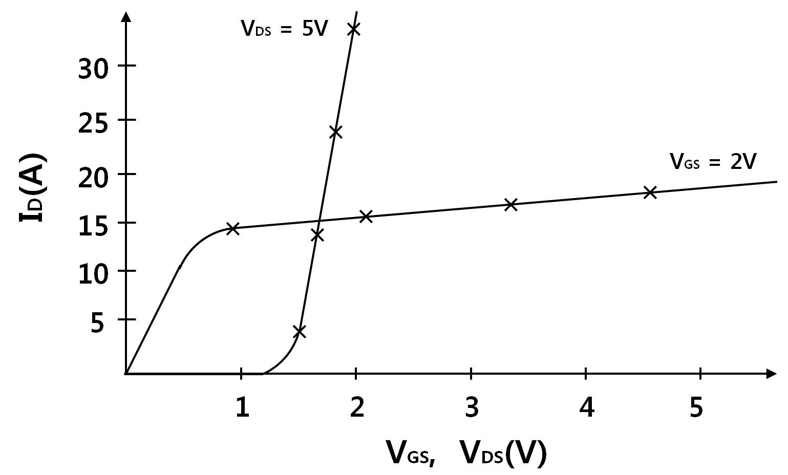
Figure 5 shows the characteristics of the drain current versus the gate and drain voltages. The threshold voltage is about 1.5 V, as obtained from the plot of the drain current versus gate voltage. The higher doping concentration in the Zener diode can increase the threshold voltage because the energy-band diagram of the MOS capacitor bends lower because of the charge trap in the channel. The induced surface potential influences the threshold voltage. For the characteristics of the current versus drain voltage
shown in Fig. 5, the on-off switching characteristics are analyzed in the triode region (VDS < 0.9 V) with a linear slope, where the drain current increases with increase of the gate voltage VGS. In the saturation region (VDS > 0.9 V), the output conductance can be obtained from the slope of the ID-VDS characteristics. The saturation output conductance is about 0.8 A/V which is a relatively large value compared to a conventional MOSFET. The conductance is not actually negligible because of the dependence of the threshold voltage on VDS or channel-length modulation. In this power MOSFET, charge sharing occurs in the source-depletion region with the gate region. Since the effective charge induced under gate reflects the charge reduction in the channel, the threshold voltage depending on the bounded charge in the depletion region will increase.
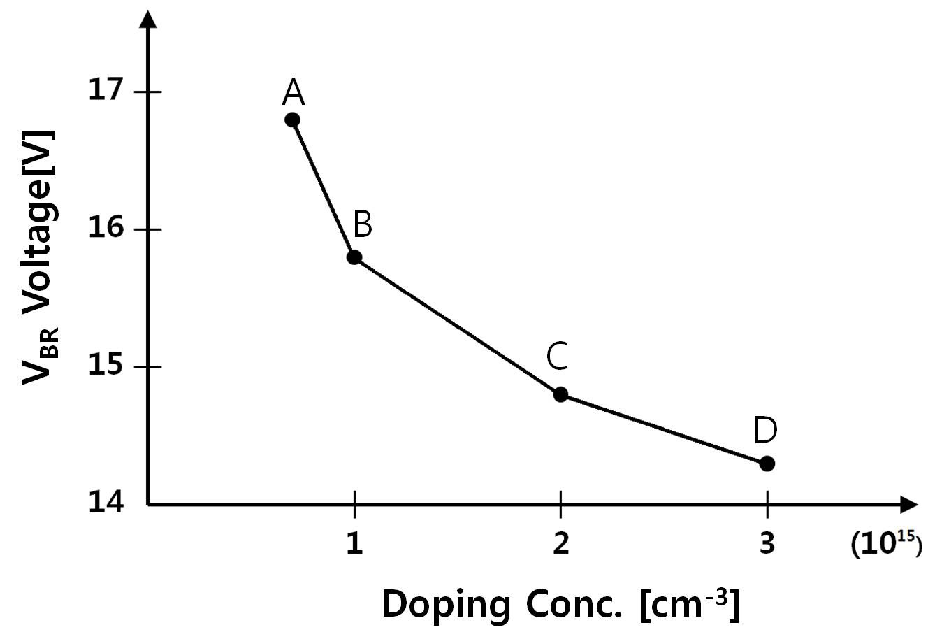
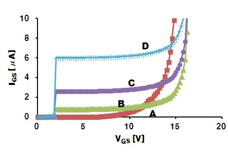
The doping concentration in the Zener diode significantly affects the breakdown voltage of the Zener diode as well as the leakage current in the power MOSFET. We defined the breakdown voltage when the gate current is over 250 μA. Figure 6 indicates that the breakdown voltage is inversely proportional to the p-doping concentration in the Zener diode. Zener breakdown occurs at the highly doped p/n junction through a tunneling mechanism. With an increase of the boron doping concentration, the valance and conduction bands on opposite sides of the junction move closer together during the bias condition in which electrons tunnel directly from the valance band.
On the other hand, the leakage current in Fig. 7 increases with higher doping concentration, where the doping concentrations A, B, C, and D are the same as those in Fig. 6. The doping concentrations A is 0.75 × 1015 cm-3. Since leakage current is sensitive to the peak longitudinal field in the channel near the gate and the drain, charge trapping here during high voltage application may distort the channel field distribution. The leakage current is shown to be in the order of μA in the characteristic of saturation. The dependency of the leakage current on doping concentration is in a trade-off relationship with that of the breakdown voltage.
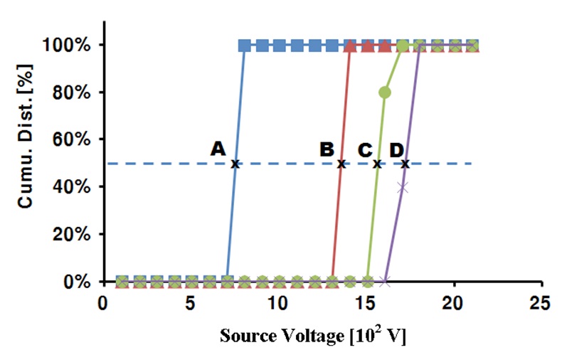
A general definition of device reliability is the probability that the device will perform a required function under stated conditions
for a stated period of time. The probability that the device will fail at or before time t is given by the cumulative distribution function. The failure drain-source voltage with the gate ground is measured by the cumulative distribution function shown in Fig. 8.
The ESD model is important to study the effect of a rechargeable battery on the human body, and is referred to as a human body model, machine model, and charge device model. In terms of device physics, the failure drain-source voltage is not useful because the gate in MOSFET usually breaks down earlier than the drain-source voltage. However, in the human body model, the short duration pulse in power MOSFET can generate a shock heat and melt aluminum metal layer. The human body model includes a 1.5 kΩ resistor and a 100 pF capacitor. Figure 8 indicates that the failure drain-source voltage in the cumulative plot is in the range of a kilo-volt and increases up to 1.7 kV at the doping concentration D. The failure voltage is defined when the leakage current is over 100 μA. The p- region in the Zener diode is connected to the N+ source through the p body region. The higher doping concentration in the p-region of the Zener diode can reduce the breakdown voltage. Therefore, a voltage which is lower than the critical voltage of the oxide under the gate is applied and improves the endurance voltage of power MOSFET. ESD protection circuit exploits only a low clamped voltage in the experiment of the power MOSFET and bypasses a strong transient voltage during the forward and reverse voltage application.
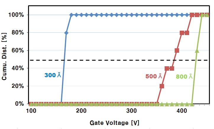
Oxide breakdown is a serious problem in power devices,. Several voltage breakdown mechanisms in MOSFET are considered, including voltage breakdown across the oxide as well as the various voltage breakdowns in the semiconductor junctions. Breakdown can occur if the electric field in the oxide sufficiently increases. In SiO2, the electric field at breakdown is on the order of 6 × 10⁶ V/cm. A safety margin is necessary since any defects that occur in the oxide can lower the breakdown field.
Figure 9 shows the failure gate voltage with variation of gate oxide thickness, which is measured with drain ground. It is obtained by the cumulative plot. The durable pulse voltage is 375 V at the oxide thickness of 500 Å. The cumulative plot at the oxide thickness of 500 Å shows a more even distribution. The failure voltage increases with increase of the oxide thickness. However, the electric field at breakdown is in the order of 7 × 10⁷ V/cm. The breakdown field is larger than that in a conventional silicon dioxide. The avalanche breakdown process is also a function of the electric field and the number of carriers involved. Avalanche breakdown near the drain terminal produces a leakage current. In this work, the failure gate voltage of the power MOSFET is the same as the breakdown voltage of the Zener diode.
The drain current of the power MOSFET is within the range of ampere, while conventional MOSFET is within the range of milli-ampere. Relatively large currents are used for the protection circuit module of rechargeable battery. The ohmic region of the MOSFET which controls the ON-OFF switching characteristic is within 1 V of the drain voltage, as shown in Fig. 5.
The drain current in the ohmic region can be written as

where K, VGS, VT ,and VDS are constant, gate voltage, threshold voltage, and drain voltage, respectively.
Another important parameter in the power MOSFET is the ON resistance, which can be written as

where Rch is the channel resistance, Rs is the resistance associated with source contact, Rd is the resistance associated with drain contact, Rsf is the resistance associated with lead frame from source to pad, and Rdf is the resistance associated with a lead frame from the drain to the pad contact. The resistance values except the channel resistance are not negligible in the power MOSFET since small resistance and high currents can induce a large amount of power dissipation. The channel resistance Rch can be written as follow, which is obtained from equation (1) with approximation of small drain voltage VDS in the triode-region of the MOSFET.

The temperature can significantly affect on K, which depends on mobility. The threshold voltage VT varies slightly with temperature. The channel resistance should be inversely proportional to the gate voltage VGS when K and VT are low in room temperature. The dependency is almost the same in the saturation region of the current-voltage characteristics.
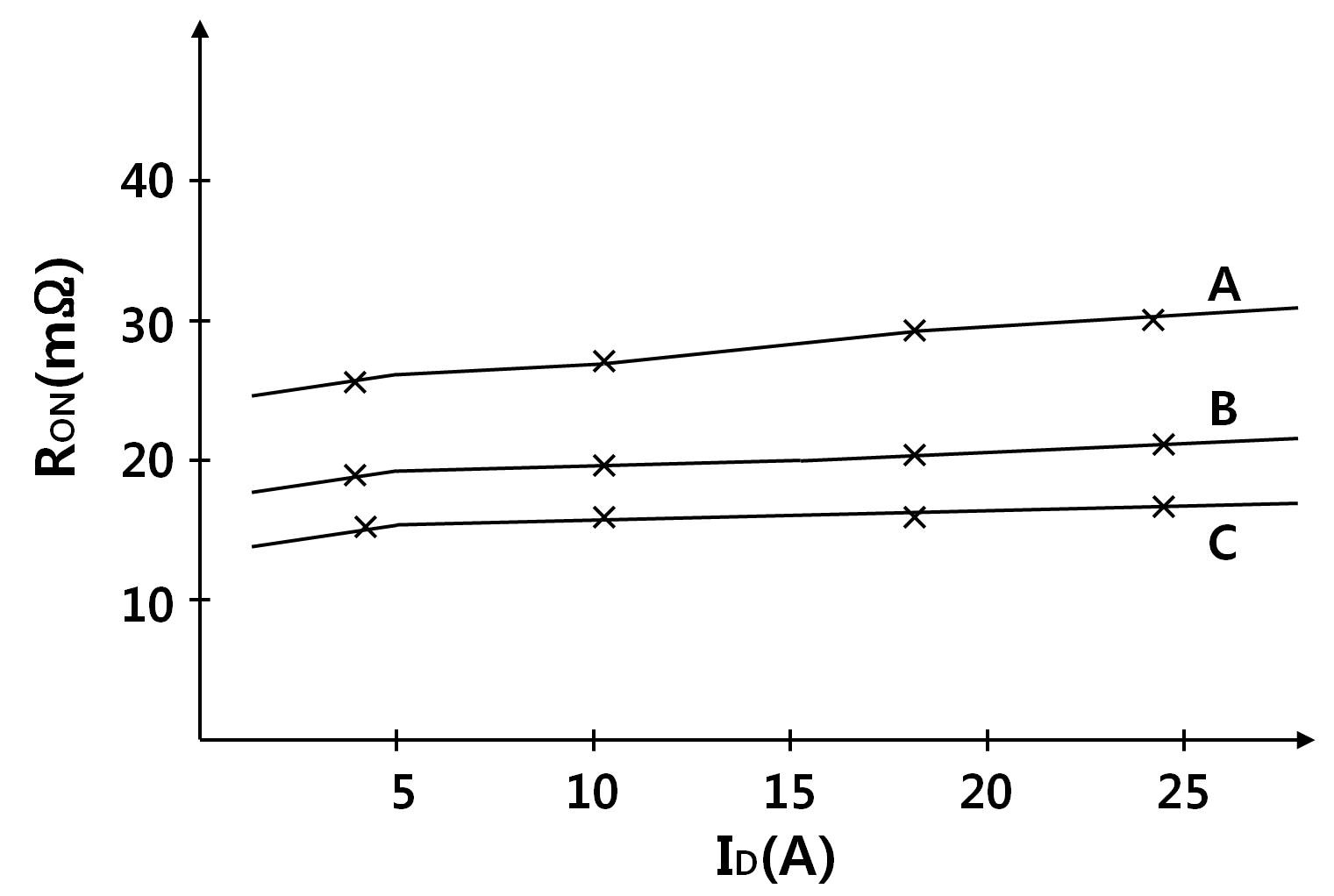
Figure 10 shows the ON resistance with variation of the drain current and gate voltage at the optimum doping concentration of 1 × 10¹⁵ (p-) and 5 × 1015 cm-3 (n+) for the p-/n+ Zener diode. The
resistance is obtained from the detection voltage of discharging over-current with the drain current of the power MOSFET. The ON resistance is shown to be inversely proportional to the gate voltage as expected and is 18 mΩ at VGS = 4.5 V and ID = 5 A. The increase in the resistance at high drain currents (> 10 A) is due to the de-biasing effect of the source parasitic resistance [8].
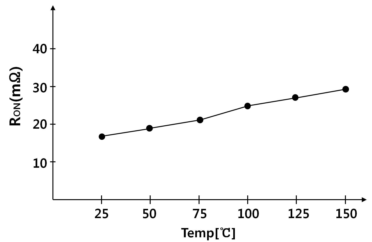
The ON resistance in this result is relatively small in the power MOSFET, of which the current capability is within the range of ampere. On the other hand, in conventional MOSFET with the current range of mA, the value of the ON resistance can be considered relatively high. Figure 11 shows the ON resistance with variation of the temperature. The resistance is shown to increase linearly with increase of temperature. At 100℃, the resistance is approximately 25 mΩ, which is almost 40% increase compared to that in room temperature. The carrier mobility increases with increase of temperature, while the threshold voltage VT changes slightly with temperature.
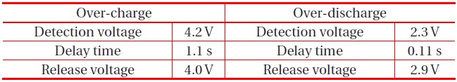
By application of the power MOSFET, protection IC module (PCM) indicates a good performance of charging characteristics, where the over-charge (over-discharge) delay time and detection voltage are controlled within 1.1 (0.11) second and 4.2 (2.3) V, respectively. Comparison with results from previous research [9] indicates a good performance of this module. Table 1 illustrates the performance of the protection IC. The electrical property of charge and discharge is obtained through the two gates in the power MOSFET as shown in Fig. 1, where the circuit parameters are shown. The other device parameters are used from the optimum condition of the power device. The high performance of protection IC derives from the fully integrated chip-module and the low ON resistance of the power MOSFET switch.
[Table 1.] Performance of the protection IC.

Performance of the protection IC.
In this paper, an integrated switching device with a Zener diode and power MOSFETs is presented for the protection circuit of a rechargeable battery. The Zener diode is integrated on top of the power MOSFET in order to protect the gate oxide from high ESD voltage. By taking into account the breakdown voltage of the Zener diode and the leakage current in the power MOSFET, an optimized doping concentration in the Zener diode is obtained, which ensures that the electrical parameters are in trade-off and the leakage current is controlled by the thickness of the gate oxide and doping concentration. The experimental result indicates that the breakdown voltage of the Zener diode and the leakage current of the power MOSFET are approximately 16 V and 1 μA respectively at the boron doping concentration of 1015 cm-3 in the Zener diode. The electrical characteristic of the MOSFET is found to be severely affected by the doping parameter in the Zener diode. In the human body model which applies a high pulse voltage in the source of the power MOSFET, the failure voltage in the cumulative plot is within the range of kilo-volt and increases with an increase of doping concentration. The ON resistance of the power MOSFET is obtained to be 18 mΩ. The low resistance provides high performance charging characteristics in the protection IC.