A volcano shaped gated Si-FEA (silicon field emitter array) was simply fabricated using sputtering as a gate electrode deposition and lift-off for the removal of the oxide mask, respectively. Due to the limited step coverage of well-controlled sputtering and the high aspect ratio in Si dry etch caused by high RF power, it was possible to obtain Si FEAs with a stable volcano shaped gate structure and to realize the restriction of gate leakage current in field emission characteristics. For 100 tip arrays and 625 tip arrays, gate leakage currents were restricted to less than 1% of the anode current in spite of the volcano-shaped gate structure. It was also possible to keep the emitters stable without any failure between the Si cathode and gate electrode in field emission for a long time.
For most applications of vacuum micro/nano electronics to devices such as electron sources and sensors [1,2], it has been highly required to develop the economical process. In spite of other merits such as size limitation, it has been required to develop silicon field emitter arrays (Si-FEAs) since all fabrication process steps are compatible with integrated circuit fabrication [3,4]. In the fabrication of micro/nano sized silicon field emitter arrays, electron gun evaporation has been mainly used as a method for the gate electrode. However, it requires a long process time as it is indispensable to heat filament [5] and it is difficult to be applied to the fabrication on the large area of substrate because it uses a point source material [6]. Therefore, the sputtering method was used as a gate electrode deposition instead of evaporation in the fabrication process of Si-FEAs [7], because it operates at relatively low pressure (about tens of mtorr) and it is possible to reduce the process time and cost.
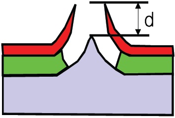
The sputtered gated Si FEAs have a shape of volcano structure caused by good step coverage of sputtering and the volcano structure has a thin and fragile edge structure caused by the shadow effect of the oxide mask. In addition, it is difficult to maintain the apex of the silicon tip as high as the edge of the gate electrode because of the good step coverage of sputtering. The electric field at the apex of the Si tip has the highest value when the tip is located as high as the gate electrode and it is necessary to optimize the structure of the volcano-shaped sputtered gated Si FEAs [8]. Figure 1 shows the volcano-shaped gated Si FEAs which are not optimized during isotropic silicon etching and subsequent oxidation to obtain the sharp tip. There is a big difference between the electrode and tip and some of the field emitted electrons may be moved to the gate electrode instead of the anode electrode. The large gate leakage current may cause a lot of power consumption and degrade reliability of Si FEAs. Up to date, the gate etchback process has been mainly used to optimize the structure of the volcano-shaped Si-FEAs [9-12]. However, it requires more process steps and process time than the lift-off process because the thickness of photo resist should be precisely controlled after hard baking and the remaining photo resist should be removed. For the stable volcano shaped structure and the restriction in gate leakage current from simply
fabricated Si FEAs with a sputtered gate, the fabrication processes were investigated and optimized. The volcano shaped Si FEAs were electrically characterized and it is expected for the Si FEAs to be easily applied to a lot of devices as a result of the low cost of fabrication and the low gate leakage.
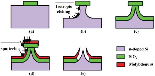
Figure 2 shows the fabrication process of sputtered gated Si-FEAs. SiO2 as thick as 4,000 Å was deposited by PECVD on phosphorus doped silicon wafer and patterned into a disk with a diameter of 1.6 ㎛ by conventional photolithography as shown in Fig. 2(a). After silicon was isotropically etched by 1.5 ㎛ at 350 W as shown in Fig. 2(b), wet oxidation was performed for 70min at 950℃ to make the emitters sharp as shown in Fig. 2(c) and thermal oxide with the thickness of 3,700 Å was obtained. Then, 1,500 Å thick molybdenum was deposited by RF sputtering at a pressure of 2.7×10⁻³ torr and at a power of 1.5 kW. As a result of sputtering in low pressure, the bottom of the oxide disk is expected to remain uncovered with molybdenum as shown in Fig. 2(d). At a low pressure, the mean free paths of Ar molecules and ions are increased because they are reversely proportional to the gas concentration and pressure [5,13]. The collisions among particles are reduced and the sputtered molybdenum atoms are expected to be controlled by the shadowing effect of the oxide disk. Therefore, the oxide disks could be easily stripped away in the buffered HF solution without any other treatment such as an ultrasonic wave. After the lift-off process was completed in the buffered HF solution for 10 min, silicon emitters became exposed as shown in Fig. 2(e).
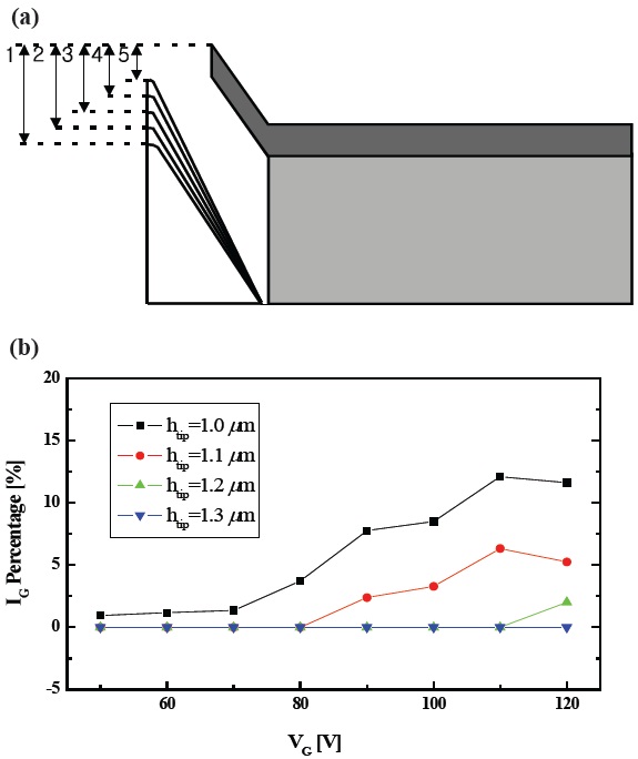
For the optimization of the volcano shaped structure in the process of Si FEAs, the structure was considered and the field emission current was calculated by using a 2-D simulator SNUFEAT [14]. Fig. 3(a) demonstrates the geometric structure of the volcano shaped field emitter used in the simulation. In Fig. 3(a), the height of the silicon tip was increased from 1 ㎛ to 1.4 ㎛. The tip radius and the thickness of the gate electrode were maintained 20 nm and 1,500 Å, respectively. Fig. 3(b) shows the portion of the gate current in the calculated field emission current for Fig. 3(a) and gate currents were obtained at the voltage of 55 V in case of the height of 1 ㎛ and at the voltage of 80 V in case of the height of 1.1 ㎛, respectively. The gate current was decreased as the Si tip was closed to the gate electrode and some emitted electrons were moved to the gate electrode instead of the anode as a result of the volcano shaped structure.
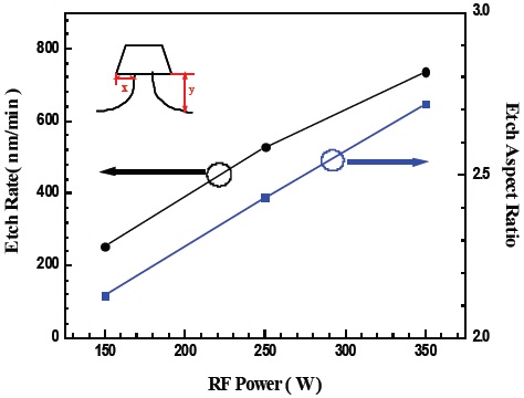
From the calculated result of Fig. 3(b), the silicon tip was optimized by means of varying etch conditions to form emitters. Silicon etch was performed by changing RF powers and keeping the other conditions such as 25 sccm SF6 and the pressure of 250 mtorr constant. Figure 4 illustrates the effects of the RF power on
the silicon etch rate and aspect ratio that is defined as the ratio of the vertical etch rate to the lateral etch rate. As shown in the figure, the silicon etch rate was increased by three times and the aspect ratio was also increased when the RF power was increased from 150 W to 350 W. Higher RF power generates more energetic ions, causing a more vertical sidewall shaped by greater physical bombardment [15]. The aspect ratios were 2.13 and 2.72 in case of 150 W and 350 W, respectively. The RF power of 350 W was used as a process condition of silicon etch in the main process. For the process condition of higher RF power, it is expected to obtain a silicon emitter with higher aspect ratio after sharpening oxidation.
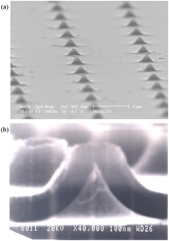
Figure 5(a) and 5(b) show a scanning electron micrograph of a fabricated Si FEA and that of the cross-sectional view of an individual field emitter, respectively. The gate hole diameter and Si tip radius of the fabricated emitter was measured at less than 500 nm and less than 10 nm from Fig. 5(b), respectively. As a result of the silicon etch with a higher RF power of 350 W and the shadow effect of the oxide mask during sputtering, the silicon tip was located lower than the gate electrode by about 1,500 Å and the gate electrode had a thin edge with a thickness of 500 Å.
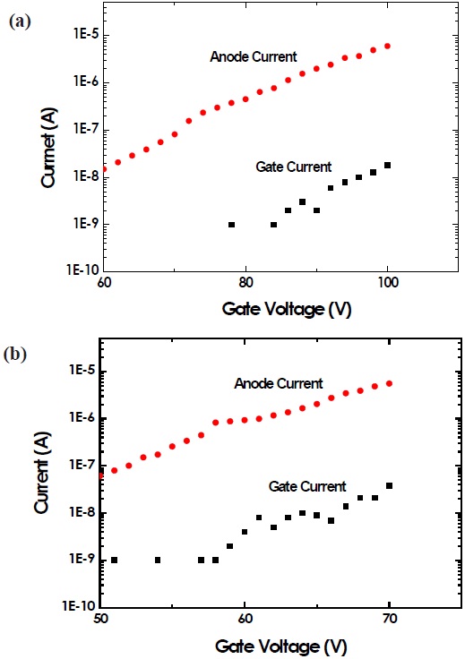
The FEAs were electrically characterized in a vacuum environment of 2×10⁻⁸ torr. Two Keithley 6487 programmable picoammeter/ voltage sources were used to apply the voltage to the gate of the FEA and the anode plate. During the measurement, the anode plate was biased at 500 V and the gate voltage was increased in the triode configuration. After a series of repeated measurement, the gate current and anode current were stabilized to reliable values. Figure 6(a) and 6(b) show the field emission
characteristics, the anode and gate current of the fabricated 100 emitter arrays and 625 emitter arrays, respectively. For the 100 emitters, an anode current of 10 nA per emitter was obtained at the voltage of 86 V. For the 625 emitters, an anode current of 10 nA per emitter is expected to be obtained at about 70 V from Fig. 6(b). The gate current of 18 nA and 38 nA were obtained at 100 V for 100 emitters and at 70 V for 625 emitters, respectively. From the difference of the gate leakage level between 100 emitters and 625 emitters, it is thought that the gate structure of the volcano shape is an element of the resistance between a silicon emitter and gate electrode and the leakage level is related to the number of emitters. From the Fig. 6(a) and 6(b), the ratio of gate current to anode current was calculated in the range from 10-3 to 3 ×10⁻³ for 100 emitter arrays and in the range from 1.2×10⁻³ to 7 ×10⁻³ for 625 emitter arrays. The gate current was maintained at less than 1% of the anode current during measurement. Since a large gate current limits the operable voltage on the gate and introduces excessive outgassing by Joule heating of both the silicon emitters and the gate electrodes [16], it is indispensable to restrict the gate current in field emitter arrays for wide applications.
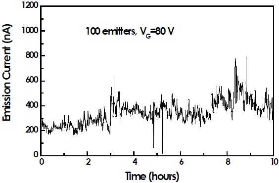
Figure 7 shows the 10 hour fluctuation of the anode current for Fig. 6(a). The gate and the anode voltages were fixed at 80 V and 300 V, respectively. The vacuum of 2×10⁻⁸ torr was maintained during the measurement. The anode current was maintained around the average value of 340 nA without any failure between the silicon emitter and gate electrode for 10 hours. It is thought that the leakage paths are barely formed between the silicon emitter and gate electrode and some protrusions and high emission points on the silicon emitter are burnt out as a result of the aging effect through some repeated measurements before the FEAs are electrically characterized.
A volcano-shaped gated Si-FEA was simply fabricated using sputtering after sharpening oxidation and its structural and electrical properties were investigated and analyzed. It was possible to obtain a stable volcano shaped gate structure and a stable anode current for an extended period of time by using the sputtering at low pressure and the isotropic properties of the Si dry etch process. The high aspect Si cathode was realized by dry etch in the condition of high RF power and the gate current was negligible compared with the anode current in spite of the volcano shaped structure because the difference in height between the Si cathode and the edge of the volcano shaped gate was reduced.