검색 전체 메뉴
PDF
맨 위로
OA 학술지
Wideband Double Dipole Quasi-Yagi Antenna Using a Microstrip-to-Slotline Transition Feed
  • 비영리 CC BY-NC
  • 비영리 CC BY-NC
ABSTRACT
Wideband Double Dipole Quasi-Yagi Antenna Using a Microstrip-to-Slotline Transition Feed
KEYWORD
Slotline Transition , Double Dipole , Tapered Coplanar Stripline
  • Ⅰ. Introduction

    Quasi-Yagi antennas are commonly used for many applications in the microwave and millimeter-wave bands because of their broad bandwidth, high gain, low cost, and high-radiation efficiency, as well as their ease of fabrication. These antennas can be fed by several types of feedlines, including microstrip lines (MS) [1]~[6], coplanar waveguides (CPW) [7], [8], coplanar striplines (CPS) [9], [10], or slotlines [11]. Quasi-Yagi antennas utilize a regular dipole as the driver, which means that the bandwidths are approximately 50 % or less and may not be sufficient for some applications. Eldek enhanced the bandwidth by introducing MS-fed planar antennas with double dipoles [12] and double rhombuses [13] as the main radiation elements. These antennas achieved a wide bandwidth with two parallel strip feedlines printed on opposite sides of the substrate. However, the radiation patterns were degraded due to the asymmetric structure of the antennas.

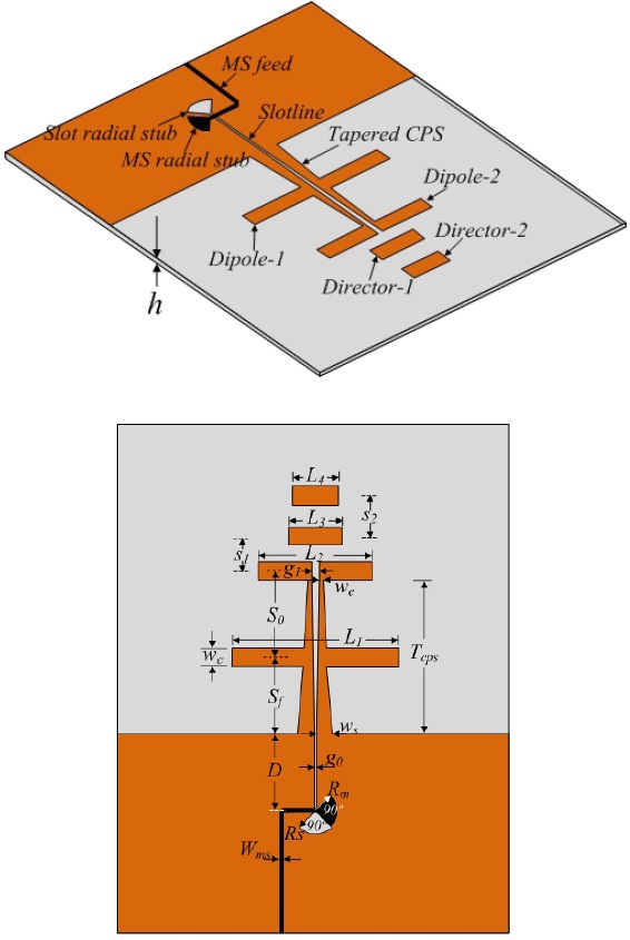
    This paper presents a microstrip-to-slotline transitionfed quasi-Yagi antenna with wide bandwidth and flat gain. The transition consists of a microstrip radial stub and a slot radial stub, each with the same 90° angle, but with different radii for impedance matching between the microstrip line and the slotline [14]. The bandwidth is enhanced by replacing the regular dipole driver with two parallel dipoles of different lengths. These double dipoles are connected to the slotline by a coplanar stripline, which is tapered to improve the impedance matching conditions. The antenna incorporates two parasitic strips as directors, and a truncated ground plane as the reflector, to achieve small gain variation across the operating bandwidth. Compared with the double dipoleYagi- Uda antenna [15], the presented antenna has a more compact and simpler structure and a wider impedance bandwidth.

    Ⅱ. Antenna Geometry

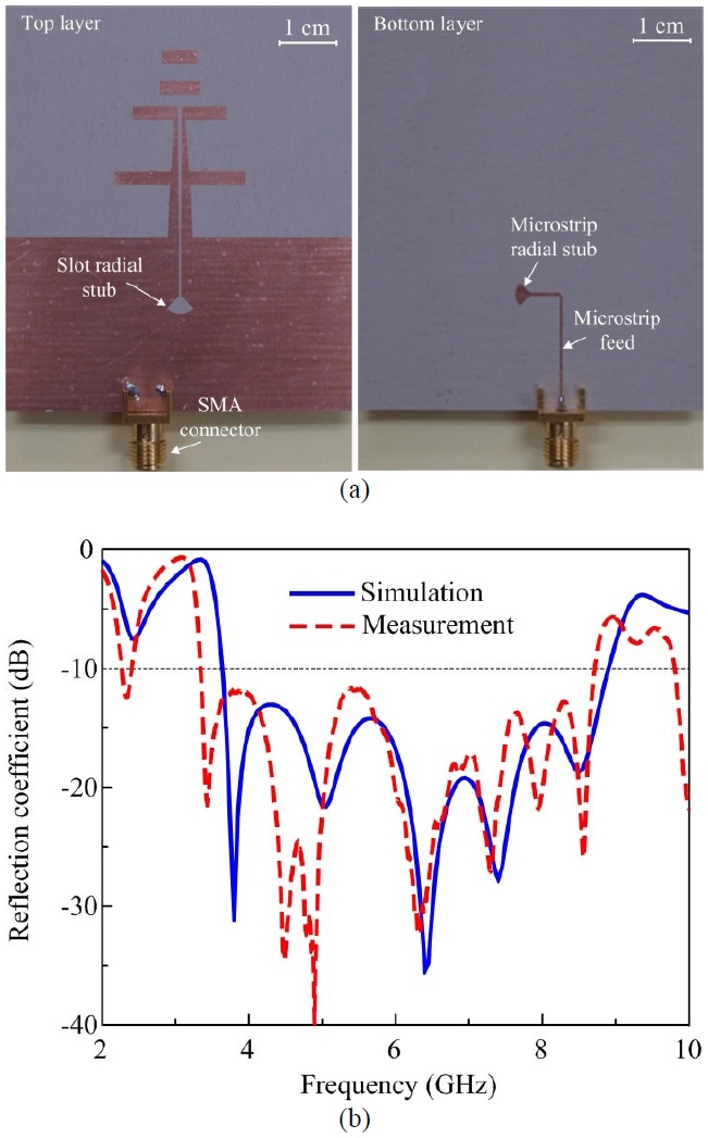
    Fig. 1 shows the geometry of the wideband microstrip- to-slotline transition-fed quasi-Yagi antenna. The antenna was designed on a 60×70 mm RT Duroid 6010 substrate with a dielectric constant of 10.2, a loss tangent of 0.0023, and a thickness of 0.635 mm. It consists of a microstrip-to-slotline transition as the feed, two parallel dipoles as the main radiation elements, two printed strips as the directors, and a ground plane as the reflector. The microstripline was designed on the back side of the substrate and had a characteristic impedance of 50 Ω. The slotline was designed with a characteristic impedance of approximately 70 Ω, due to a compromise between the narrow slot width required to obtain a characteristic impedance of 50 Ω and the limitations of the available fabrication technique. Therefore, a microstrip radial stub and a slot radial stub, each having the same angle of 90° but with different radii, were inserted into the transition to provide impedance matching between the microstrip-line and the slotline. Two parallel dipoles acted as the primary radiation elements, which were directly connected to the slotline by a coplanar stripline. The initial lengths of dipole-1 and dipole-2 were approximately one-half of the effective wavelengths (λeff/2) at 4 and 6.5 GHz, respectively. However, the input impedance of the double dipoles is higher than the characteristic impedance of the slotline and the input impedances at each dipole are different. Therefore, the coplanar stripline was shaped from a wide-line width with a smallgap to a narrow-line width with a largegap to improve the impedance matching condition. Additionally, two dipoles were arranged to minimize the gain variation in the low-frequency region (3.5~6.5 GHz) with the dipole-1 to reflector (ground plane) spacing of Sf and the dipole-1 to dipole-2 spacing of S0. The directors were designed to have a resonance near 8.5 GHz and to achieve an optimal phasing for a small gain variation in the high-frequency region (6.5~9 GHz). The antenna characteristics were investigated with an Ansoft high-frequency structure simulator (HFSS) and the optimized antenna design parameters are given in Table 1. The next section is a parametric study that shows the effects of several main design parameters on the antenna characteristics.

    [Table 1.] Optimized antenna design parameters.

    label

    Optimized antenna design parameters.

    Ⅲ. Parametric Study

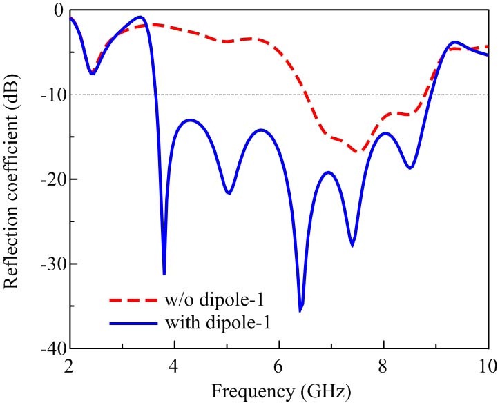
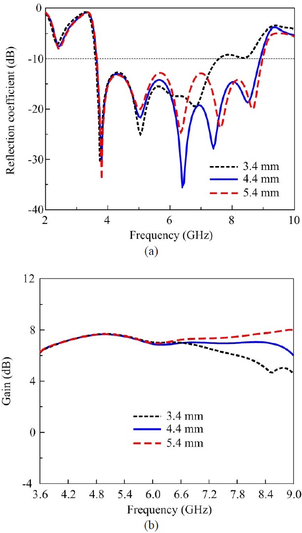
    As mentioned before, the key motivation for the use of two parallel dipoles is to achieve multi-resonances, and consequently, to further enhance the bandwidth. This is clearly observed in Fig. 2, which shows the simulated reflection coefficient of the antenna with/without dipole-1 (L1). In the absence of dipole-1, the antenna exhibited three-resonances around 6.6, 7.4, and 8.4 GHz, and the bandwidth was 6.55~8.75 GHz for a ?10 dB reflection coefficient. In the presence of dipole- 1, the antenna showed five-resonances around 3.8, 4.5, 6.3, 7.3, and 8.4 GHz, and the bandwidth was 3.65 ~8.90 GHz for the ?10 dB reflection coefficients. The impedance bandwidth of the microstrip-to-slotline transition fed quasi-Yagi antenna was enhanced from 29 % to 83.7 % by the use of double dipoles as the primary radiation elements.

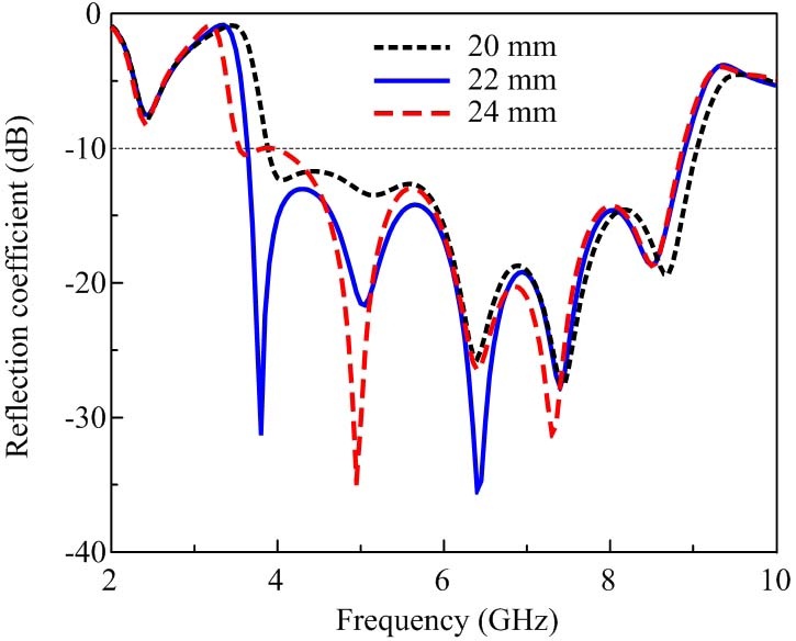
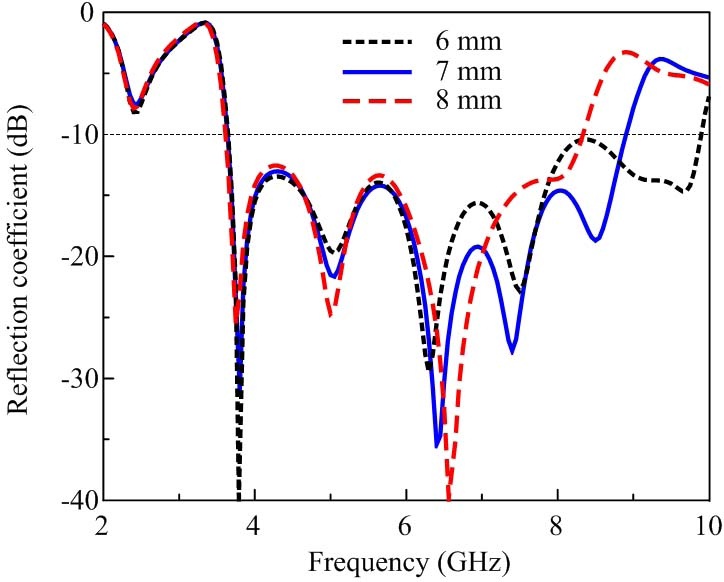
    Fig. 3 shows the simulated reflection coefficient as a function of frequency for different lengths of dipole-1 (L1). As L1 was increased from 20 mm to 24 mm in 2 mm steps, the lowest resonant frequency decreased while other resonances changed only slightly. Fig. 4 shows the simulated reflection coefficient as a function of frequency for different lengths of the dipole-2 (L2). As L2 was increased from 14 mm to 18 mm in 2-mm-steps, the third resonance (near 6.3 GHz) decreased but other resonances hardly changed. Fig. 5 shows the antenna reflection coefficient as a function of frequency for different lengths of the director-1 (L3). As L3 was increased from 6 mm to 8 mm in 1 mm steps, the resonances in the high-frequency region decreased, while the resonances in the low-frequency region remained almost the same. These results indicate that the lengths of L1~3 mainly determine the resonances of the antenna. The effect of these parameters on the antenna gain is negligible and is not shown here.

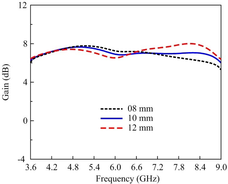
    This study also investigated the antenna design parameters that negligibly affect the reflection coefficient (not shown), but strongly influence the gain. Fig. 6 shows the simulated gain as a function of frequency for different spacings between the ground plane and longer dipole (Sf). As Sf was varied from 8 mm to 12 mm in 2-mm-steps, the gain degraded in the low-frequency region, but improved in the high-frequency region. Fig. 7 shows the simulated gain as a function of frequency for different spacing between two parallel dipoles (S0). As S0 was varied from 9.2 mm to 13.2 mm in 2 mm steps, the gain slightly improved in the low-frequency region (3.6~4.8 GHz), but was significantly degraded in the high-frequency region. These results indicate that the gain of the proposed antenna can be controlled by adjusting Sf and S0.

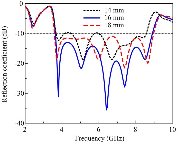
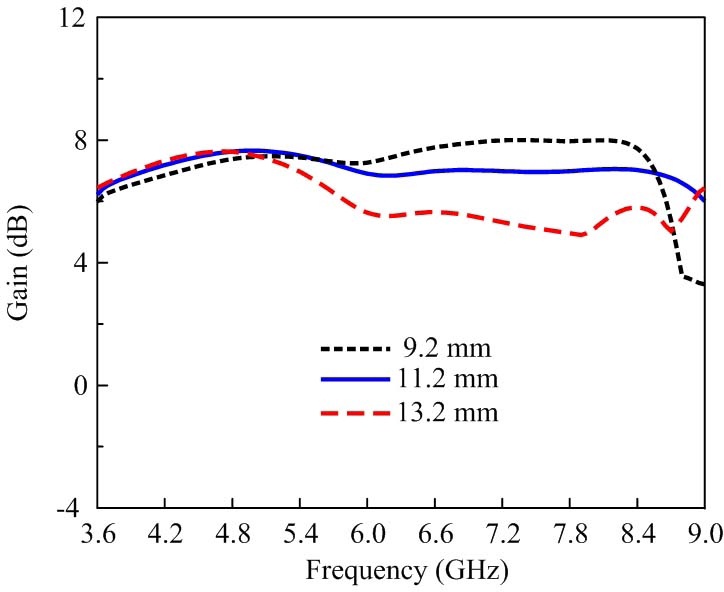
    Fig. 8 shows the variations in the antenna characteristics as a function of frequency for different spacings between the shorter dipole and director-1 (S1). Increments of 1 mm in this space, from 3.4 mm to 5.4 mm, induced significant changes in the reflection coefficient and gain in the high-frequency region but negligible changes in low-frequency region. This indicates that the space between the parallel dipoles and the directors mainly affects the antenna characteristics in the highfrequency region.

    Ⅳ. Simulation and Measurement Results

    The antenna was fabricated on both sides of an RT/Duroid 6010 substrate with a 20-μm copper thickness, and a subminiature type-A (SMA) connector was used as a microstrip-to-coaxial line transition (not included in HFSS simulations). An Agilent N5230A network analyzer and an Agilent 3.5-mm 85052B calibration kit were used for measurements of the prototype [Fig. 9(a)]. As shown in Fig. 9(b), the measured and simulated reflection coefficients of the antenna agreed rather closely. The measured bandwidth was 3.34~8.72 GHz for the ?10 dB reflection coefficient while the simulated bandwidth was 3.65~8.9 GHz. The slight difference between the measured and simulated results could be attributed to a misalignment at the transition and the effect of the SMA connector.

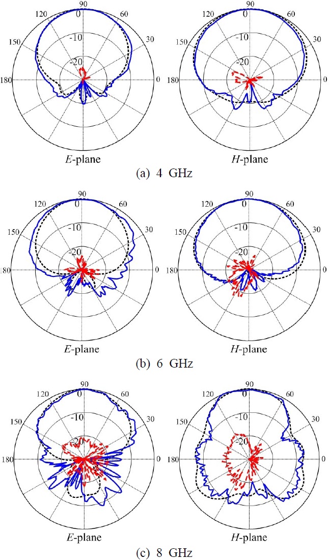
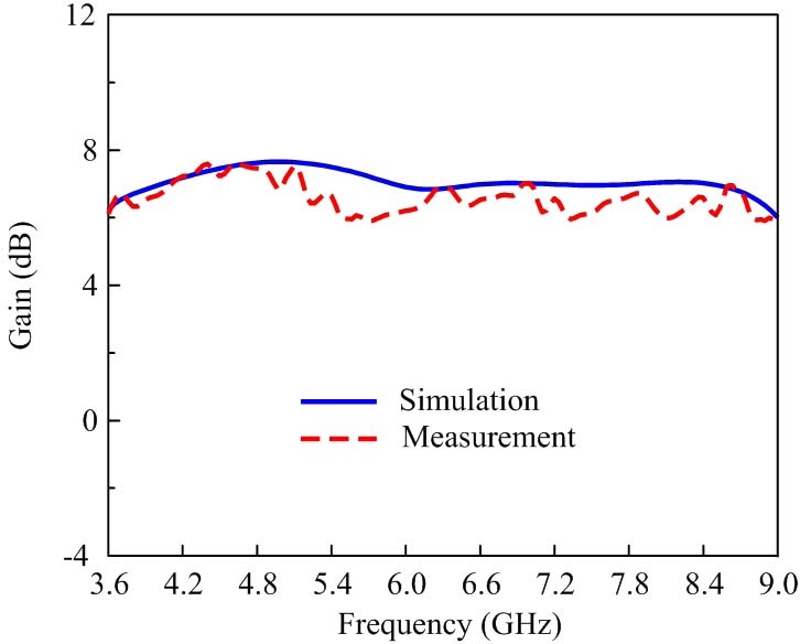
    The normalized radiation patterns of the antenna at 4, 6, and 8 GHz are illustrated in Fig. 10, and showed a good agreement between the measurements and simulations. The radiation patterns are symmetric and stable, with a front-to-back ratio and cross-polarization level better than 15 and ?17 dB, respectively. At a frequency of 4 GHz, the measurements resulted in a half power beamwidth (HPBW) of 83° and 113° along the E- and H-planes, respectively. At 6 GHz, the measurements resulted in a HPBW of 92° along both E- and H-planes. At 8 GHz, the measurements resulted in a HPBW of 83° and 77° along the E- and H-plane, respectively. As shown in Fig. 11, the measured gain of the antenna was 6.3~7.5 dBi across the bandwidth, which agreed closely with the simulated gain of 6.4~7.6 dBi. Some ripples in the measured results could be attributed to scattering effects arising fromrement setup. The antenna also exhibited a relatively small gain variation (±0.6 dB) at 3.6~9 GHz; thus, it can be used for transmitting or receiving applications in wideband wireless communication systems.

    Ⅴ. Conclusion

    This paper introduced a microstrip-to-slotline transition- fed quasi-Yagi antenna with a wide bandwidth and a flat gain. Wideband characteristics and stable radiation patterns were achieved by replacing the regular dipole driver with two parallel dipoles of different lengths, which were directly connected to the slotline by a tapered coplanar stripline. The planar structure, stable radiation pattern, wideband characteristics (3.34~8.72 GHz), small gain variation (6.9±0.6 dBi), low cross-polarizations (<?17 dB), and high front-to-back ratio (>15 dB) of the proposed antenna make it widely applicable to wideband wireless communication systems.

참고문헌
  • 1. Qian Y., Deal W. R., Kaneda N., Itoh T. 1998 "Microstrip fed quasi-Yagi antenna with broadband characteristics" [Electron. Lett.] Vol.34 P.2194-2196 google
  • 2. Zheng G., Kishk A. A., Glisson A. W., Yakovlev A. B. 2004 "Simplified feed for modified printed Yagi antenna" [Electron. Lett.] Vol.40 P.464-466 google
  • 3. Woo D. S., Kim Y. G., Kim K. W., Cho Y. K. 2008 "Design of quasi-Yagi antennas using an ultra-wideband balun" [Microw. Opt. Tech. Lett.] Vol.50 P.2068-2071 google
  • 4. Ta S. X., Kim B., Choo H., Park I. 2011 "Design of broadband quasi-Yagi antenna using a folded dipole driver" [JKIEES] Vol.11 P.227-233 google
  • 5. Ta S. X., Kim B., Choo H., Park I. 2012 "Wideband quasi-Yagi antenna fed by microstrip-to-slotline transition" [Micro. Opt. Techn. Lett.] Vol.54 P.150-153 google
  • 6. Ta S. X., Kang S., Park I. 2012 "Closely spaced twolement folded-dipole-driven quasi-Yagi array" [J. Electromagn., Eng. Sci.] Vol.12 P.254-259 google
  • 7. Kan H. K., Waterhouse R. B., Abbosh A. M., Bialkowski M. E. 2007 "Simple broadband planar CPWed quasi-Yagi antenna" [IEEE Antenna Wireless Propag. Lett.] Vol.6 P.18-20 google
  • 8. Truong L. H., Baek Y. H., Lee M. K., Park S. W., Lee S. J., Rhee J. K. 2009 "A high-performance 94 GHz planar quasi-Yagi antenna on GaAs substrate" [Microw. Opt. Tech. Lett.] Vol.51 P.2396-400 google
  • 9. Han K., Park Y., Choo H., Park I. 2009 "Broadband CPS-fed Yagi-Uda antenna" [Electron. Lett.] Vol.45 P.1207-1209 google
  • 10. Alhalabi R., Rebeiz G. 2010 "Differentially-fed millimeter- wave Yagi-Uda antennas with folded dipole feed" [IEEE Trans. Antenna Propag.] Vol.58 P.966-969 google
  • 11. Ta S. X., Kim B., Choo H., Park I. 2010 "Slotine-fed quasi-Yagi antenna" [International Symposium on Antennas, Propagation, and EM Theory] P.307-310 google
  • 12. Eldek A. A. 2006 "Design of double dipole antenna with enhanced usable bandwidth for wideband phase array applications" [Progress in Electromagnetics Research] Vol.59 P.1-15 google
  • 13. Eldek A. A. 2007 "Ultrawideband double rhombus antenna with stable radiation patterns for phased array applications" [IEEE Trans. Antenna Propag.] Vol.55 P.84-91 google
  • 14. Zinieris M. M., Sloan R., Davis L. E. 1998 "A broadband microstrip-line-to-slot-line transition" [Microw. Opt. Tech. Lett.] Vol.18 P.339-342 google
  • 15. Ta S. X., Choo H., Park I. 2012 "Wideband double- dipole Yagi-Uda antenna fed by a microstriplot coplanar stripline transition" [Progress in Electromagnetics Research B] Vol.44 P.71-87 google
OAK XML 통계
이미지 / 테이블
  • [ Fig. 1. ]  Geometry of the wideband double dipole quasi-Yagi antenna.
    Geometry of the wideband double dipole quasi-Yagi antenna.
  • [ Table 1. ]  Optimized antenna design parameters.
    Optimized antenna design parameters.
  • [ Fig. 2. ]  Simulated reflection coefficient of the antenna with/without dipole-1.
    Simulated reflection coefficient of the antenna with/without dipole-1.
  • [ Fig. 3. ]  Simulated reflection coefficient as a function of the dipole-1 length (L1).
    Simulated reflection coefficient as a function of the dipole-1 length (L1).
  • [ Fig. 4. ]  Simulated reflection coefficient as a function of the dipole-2 length (L2).
    Simulated reflection coefficient as a function of the dipole-2 length (L2).
  • [ Fig. 5. ]  Simulated reflection coefficient as a function of the director-1 length (L3).
    Simulated reflection coefficient as a function of the director-1 length (L3).
  • [ Fig. 6. ]  Simulated gain as a function of the space between the ground plane and double dipoles (Sf).
    Simulated gain as a function of the space between the ground plane and double dipoles (Sf).
  • [ Fig. 7. ]  Simulated gain as a function of the space between two parallel dipoles (S0).
    Simulated gain as a function of the space between two parallel dipoles (S0).
  • [ Fig. 8. ]  (a) Simulated reflection coefficient and (b) gain as a function of the spacing between the double dipoles and director (S1).
    (a) Simulated reflection coefficient and (b) gain as a function of the spacing between the double dipoles and director (S1).
  • [ Fig. 9. ]  (a) Fabricated wideband double dipole microstripto- slotline transition fed quasi-Yagi antenna, (b) measured and simulated reflection coefficient.
    (a) Fabricated wideband double dipole microstripto- slotline transition fed quasi-Yagi antenna, (b) measured and simulated reflection coefficient.
  • [ Fig. 10. ]  Normalized radiation patterns of the antenna: ----- co-polarization simulation, ----- co-polarization measurement, and ---- cross-polarization measurement. Simulated cross-polarization is excluded because value is too small to show in Figure.
    Normalized radiation patterns of the antenna: ----- co-polarization simulation, ----- co-polarization measurement, and ---- cross-polarization measurement. Simulated cross-polarization is excluded because value is too small to show in Figure.
  • [ Fig. 11. ]  Gain of the optimized antenna.
    Gain of the optimized antenna.
(우)06579 서울시 서초구 반포대로 201(반포동)
Tel. 02-537-6389 | Fax. 02-590-0571 | 문의 : oak2014@korea.kr
Copyright(c) National Library of Korea. All rights reserved.