In a synchronous digital system, the clock signal is used to define a time reference for the movement of data in the system. The clock distribution network distributes the clock signal(s) from a clock source to all sequential elements which require it. Thus, the clock function is vital to the operation of the synchronous system. Nowadays, much more attention has been paid to clock related design than ever before. This is because as the clock frequency increases over a 1 GHz with low supply voltage, a small noise on the clock signal causes a transient function error or even a drastic system failure (the noise comes from many factors such as current charge/discharge variation and temperature variation). One of the most important clock design issues is analyzing the clock signals’ behavior, and mitigating the adverse impact of clock noise on circuit reliability.
This work overviews a number of important clock network optimization problems and the proposed techniques with regard to the circuit reliability in deep submicron design technology. The following subsections cover 1) the clock polarity assignment problem for reducing peak current noise on the clock tree, 2) the clock mesh network design problem for tolerating the clock skew variation, 3) the electromagnetic interference (EMI) aware clock optimization problem, 4) the adjustable delay buffer (ADB) allocation and assignment problem that is useful in the multiple voltage modes design environment and finally 5) the finite state machine (FSM) state encoding problem for reducing peak current in the sequential elements in FSM. Note that the last topic is not directly related to the clock design issue, but it can be regarded that reducing noise at the activation of sequential elements driven by a clock signal is contained within the spectrum of achieving reliable circuits from the clock source down to sequential elements.
II. CLOCK TREE SYNTHESIS OVERVIEW
A typical clock tree synthesis (CTS) process consists of three phases: abstract tree topology generation, clock tree routing, and buffer insertion.
Fig. 1 shows the flow of the methods of means and medians (MMM) algorithm [1]. It takes the clock sink locations as input and generates an abstract clock tree topology by recursively partitioning the sinks into two subregions until there are at most two sinks on each subregion. The partitions are performed either in the x direction or y direction, dividing the number of sinks equally using the concept of median. The partitions are then merged back in reverse order, forming an abstract tree topology where the merging points are determined using the concept of mean (i.e., center of mass) of the sink locations on the subregions to be merged. The more accurate determination of the location of merging points (i.e., the internal nodes of tree) is performed in the wire routing step.
With the abstract topology obtained, the actual wire routing from the clock source toward the sinks is accomplished by other algorithms. One of the most notable algorithms is the deferred merge embedding (DME) algorithm [2,3], which ensures zero clock skew while mini-
mizing the total clock wire length (the clock skew refers to the delay difference between the earliest arrival time and latest arrival time to sinks). The DME algorithm runs in two stages; one is a bottom-up process from sinks and the next is a top- down process from the root of clock tree.
Fig. 2a and b show the bottom-up stage in which the algorithm builds
The final step of CTS is to insert buffers into the clock tree. The clock slew-rate, which is the sharpness of the clock signal voltage rise and fall, must be controlled in modern chip design. With large clock trees, the wire capacitance is too large to be driven by one large buffer placed at the root of the clock tree. Hence, buffers need to be inserted into the clock tree to meet both the slew and skew constraints. Many works have combined the first
two phases with the buffer insertion [4-6].
Recently, some works attempted to integrate circuit simulation into the CTS process while trading off between the accuracy of the delay model and the quality of CTS [7]. On the other hand, instead of sacrificing simulation time with CTS quality, some approaches have proposed the adaptation of the independent delay model. This is accomplished by carefully constructing clock trees to have a symmetrical structure that guarantees zero clock skew throughout the clock tree. Shih and Chang [8] met near the zero skew (<2.1 ps) goal while achieving orders of magnitude runtime speedup.
III. RELIABILITY AWARE CLOCK DESIGN TECHNIQUES
>
A. Clock Polarity Assignment
In synchronous circuits, clock trees and its clocked loads are the major sources of on-chip noise (power/ ground voltage fluctuations) since they switch simultaneously near the rising and/or falling edge of the clock signal and draw a significant amount of current from the power/ground rail. To accommodate this simultaneous switching, Vittal et al. [9] and Vuillod et al. [10] took advantage of clock skew to scatter the clock signal arrival times along the time domain.
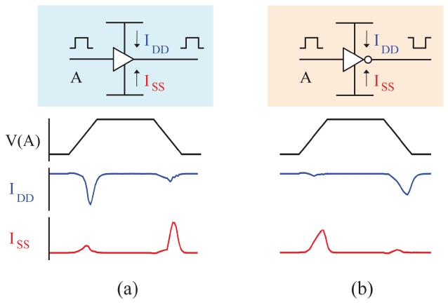
Thereafter, Nieh et al. [11] introduced additional flexibility to this scattering, by firstly proposing the polarity assignment technique. They demonstrated that mixing buffers and inverters for clock buffering elements can disperse noise over rising and falling edges of the clock as shown in Fig. 3. The approach assigned half of the buffering elements to a negative polarity and the other half positive by replacing one of the two buffers that are connected to the clock source with an inverter. However,
although the total peak current is significantly reduced, since power/ground noise is a local effect, the problem remained largely unsolved. Samanta et al. [12] mixed buffers and inverters throughout the clock tree structure so that for each local region about half of the buffering elements have positive polarity and the other half negative polarity. This approach, however, while greatly reducing noise, is likely to introduce large clock skew. According to more recent data [13], mixing buffers and inverters for non-leaf elements resulted in an average clock skew of 592 ps. Chen et al. [14] observed that noise from leaf buffering elements dominates that from non-leaf buffering elements. This phenomenon is more prominent when the clock tree is not a binary tree where one non-leaf buffering element has more than two leaf buffering elements attached. Hence, they proposed to assign polarity to leaf buffering elements only and assigned half of the leaf nodes to negative polarity, with the objective of minimizing clock skew. However, this approach only heuristically solved the noise reduction problem in that it does not consider the buffer load which affects the peak value of the noise current. Jang et al. [15] proposed and solved a combined problem of buffer sizing and polarity assignment with the proof of the nondeterministic polynomial time (NP)-completeness of the polarity assignment problem. It retrieves all assignment combinations under the clock skew constraint and selects the one with the lowest noise. Very recently, Joo and Kim [16] proposed a finegrained polarity assignment to overcome the two limitations of the prior works, which are the unawareness of the signal delay (i.e., arrival time) differences to the leaf buffering elements and the ignorance of the effect of the current fluctuation of non-leaf buffering elements on the total peak current waveform.
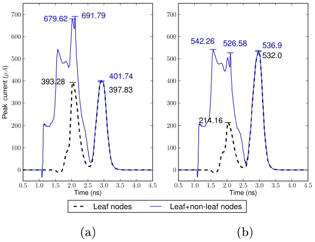
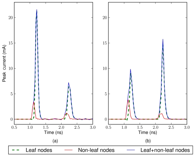
Fig. 4 illustrates the difference between non-leaf blind and non-leaf aware polarity assignments. In Fig. 4a, the black dotted line which is the current waveform from leaf nodes is well balanced, indicating that the noise is minimized for the leaf nodes. However, the solid line with blue color which is the total noise waveform of both the leaf nodes and the non-leaf nodes is not balanced. The combined noise causes a higher peak current value than the original expectation that comes from the consideration of leaf nodes only. Fig. 4b shows an improved result in which the non-leaf noise is considered. At leaf nodes, more current noise is migrated to the falling edge of the clock signal, yielding a greater margin for the non-leaf node noise. The results of Fig. 4 suggest that polarity assignment algorithms need to consider the effect of the noise caused by non-leaf nodes on the leaf nodes, even when only assigning polarity to the leaf nodes only.
Fig. 5 compares the polarity assignment results by Jang and Kim’s algorithm [15] and Joo and Kim’s finegrained approach [16]. Joo and Kim’s modeling captured more details of the noise waveform, including smaller bumps at the opposite clock edge of the larger peak noise,
arrival time differences, and non-leaf element noise. Thus, more of the buffering elements were assigned as inverters, showing better balanced noise levels at the rising and falling edge of the clock.
In addition, there are a number of works which have considered other design factors to improve the quality of polarity assignment. Kang and Kim [17] considered a statistical delay variation to increase yield during polarity assignment. Ryu and Kim [18] took a different approach by assigning polarity to leaf nodes first and then routing the clock tree. Lu and Taskin [19] exploited exclusive-or
(XOR) gates, instead of inverters and buffers, so that polarity may be controlled at runtime.
>
B. Clock Mesh Network Design
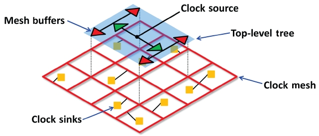
As complementary metal-oxide-semiconductor (CMOS) process scaling continues under deep submicron technology while clock frequency increases, the variation effect on clock skew becomes significant. It is known that the delay variation on the interconnect can cause up to 25% variation in clock skew [20], implying the necessity of controlling the variation effect during the clock network design. The mesh-based clock distribution network, as depicted in Fig. 6, is one of the solutions that can effectively mitigate the clock skew variation since multiple paths from the clock source to a sink are able to compensate the different clock arrival times.
However, the multiple paths are likely to generate short circuit currents between mesh buffers which have different clock arrival times. Moreover, the mesh-based clock network requires much more wires than the treebased clock network in order to support multiple clock signal paths. Consequently, most of related works have focused on reducing the amount of power consumption and wire resource while maintaining clock skew variation tolerance. Venkataraman et al. [21] decided the location and size of buffers first, and then reduced mesh wires; they solved the mesh buffer placement and sizing problem by formulating it into a weighted set-cover problem. Precisely, for each node (i.e., buffer) in the clock mesh they defined a so called covering region, which refers to the set of nodes that the node can drive. Subsequently, they locate a minimal set of covering regions that can cover all nodes in the clock mesh. They employed a greedy algorithm which iteratively picks a covering region that covers the largest number of uncovered nodes. The mesh reduction problem was then solved by formulating it into the Steiner network problem [22]; they iteratively removed wire segments while maintaining a certain level of redundancy, i.e., every clock sink should have at least
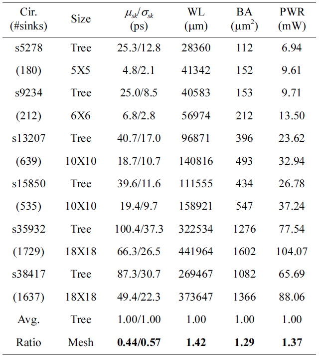
To demonstrate the variation tolerance of the clock mesh, we compare the clock mesh with the clock tree in terms of the clock skew and resource usage. We implemented the clock mesh with a given mesh size and inserted buffers by using the algorithm of buffer placement and sizing in [21]. Then, the clock trees are generated by applying the algorithm in [3,6]. We tested clock meshes and clock trees on ISCAS89 benchmark circuits. We used 12 buffer sizes with maximum-capacitance ranging from 60 to 500 fF under a slew constraint of 100 ps. The technology parameters and transistor models were based on 45 nm predictive technology [24]. We consider 4 variation parameters: power supply voltage, buffer channel length, wire width, and sink capacitance. All variation parameters are varied with 5% standard deviation around its nominal value. We also consider the spatial correlation by the principal component analysis [25]. The columns in Table 1 are benchmark circuit name, given mesh size (‘Tree’ for the result of clock tree), mean and standard deviation of the clock skew (measured by HSPICE Monte-Carlo simulations), total wirelength (WL), buffering area (BA), and power consumption (PWR). The last two rows in Table 1 are the average ratio of clock trees and clock meshes. Table 1 indicates that the clock mesh can reduce 50% of worst-case clock skew (
>
C. Electromagnetic Inference Aware Clock Design
Increasing the requirement for high performance circuits and the enforcement of strict governmental regulation leads to a new design solution for EMI. Electromagnetic radiation from an electronic circuit can be categorized into two forms [26]:
EMI-aware clock optimization is a clock network synthesis method with the objective of reducing EM emis-

Comparison of clock tree and clock mesh in terms of clock skew, wire length (WL), buffer area (BA), power consumption (PWL)
emission by controlling clock parameters. The key clock parameters are slew rate and clock skew. Slew rate is the rise/fall time in the clock signal which typically has a trapezoidal waveform. With Spectral analysis, the clock signal can be represented in the sum of series regarding sine and cosine functions. The amplitude of high frequency functions critically depends on the speed of slew rate [27]. In other words, a clock signal with a fast slew rate has larger amplitude in high frequencies compared to those with a slower slew rate. Previous works demonstrate that in order to reduce total EMI it is very effective to decrease the slew rate of the clock signal [27-29]. Pandini et al. [27] proposed a method to decrease the slew rate by manually removing buffers and inverters with higher driving strength from the target library. Hu and Guthaus [29] proposed a method of weakening buffer driving strength by setting the constraint of minimum slew rate during clock tree synthesis. They proposed an incremental dynamic programming algorithm to determine buffer sizing and positioning for a clock tree, considering metrics such as skew and power used in [27]. EM emission is also primarily generated by simultaneous switching noise (SSN). In the clock network, sink buffers and connected flip-flops toggle almost at the same time, creating a large current pulse on the power network, and fast current variation increases di/dt, causing a high SSN. Note that peak current can be controlled by spreading the activity of buffers and flip-flops within a time period, but it causes a clock skew variation. Vuillod et al. [10] pro-posed a solution to reduce peak current by relaxing the clock skew constraint. Pandini et al. [27] performed a theoretical analysis on power/ground noise by describing noise using a periodic triangular pulse, and demonstrated that increasing skew bound is effective in reducing EM emission.
>
D. Adjustable Delay Buffer Allocation
Traditional clock optimization techniques are mainly based on the environment in which all elements in a circuit use one fixed operating voltage. However, a recent technological trend requires multiple supply voltages to allow the voltage level applied to a circuit to be dynamically changed. In this multi-voltage mode design, some part of the circuit could operate at high voltage when the associated module is required to complete its processing quickly and at low voltage when timing requirement can be relaxed and reducing power is more important. When the supplied voltage switches from high to low (or low to high), the delay of all logic elements including buffers in the clock network on the part of the chip also varies. One serious problem in this multi-voltage mode design is the clock skew variation on the clock network.
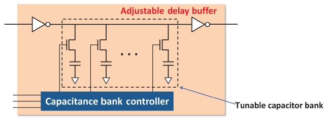
To tackle the clock skew variation problem, Su et al. [30] proposed a methodology of dealing with clock skew optimization in which they proposed using ADB, which is a specially designed buffer so that its delay can be controlled dynamically. The general structure of ADB is shown in Fig. 7. It is composed of a normal buffer, internal capacitor bank, and a capacitor bank controller. The delay of ADB could be adjusted by activating the internal capacitor bank. That is, the adjusted delay of ADB is determined by the amount of activated capacitors in the capacitor bank that is controlled by the capacitor bank controller and its control input.
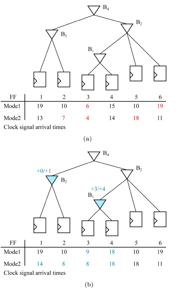
Fig. 8 demonstrates how ADBs can be used to fix clock skew violations. In Fig. 8a, an initial clock tree with clock signal arrival times for each clock sink in two power modes is given. With the clock skew bound of 10, there is one clock skew violation between FF1 and FF6 in power mode 1. By replacing buffer B1 with an ADB and inserting an additional delay of 3, this violation can be fixed. For power mode 2, there are two violations, one between FF3 and FF6 and the other between FF2 and FF6. By allocating ADBs at B1 and B3 and assigning their delay values with 4 and 1, respectively, the clock skew violation is removed. The resulting ADB allocation is shown in Fig. 8b.
The problem to be solved in using ADBs in a multivoltage mode design is to minimize the cost of ADBs to be used since an ADB has more transistors than a normal buffer due to the internal capacitor bank and controller. The approach in [30] focused on the power mode with the worst violation of the clock skew constraint and resolved the worst clock skew by adding ADBs in a greedy man-
ner. The approach was then repeated until there was no clock skew violation for every power mode. While the approach can efficiently find an ADB allocation with no clock skew violation, an optimal ADB allocation is not guaranteed due to the inherent limitation induced by the iterative heuristic. Later on, Lim and Kim [32] improved the work in [30] by proposing a linear time optimal algo-rithm for the ADB allocation and delay value assignment. Initially, they replaced all buffers in the clock tree with ADBs and then removed unnecessary ADBs through a comprehensive analysis of the timing relation between ADBs. They performed the analysis in a bottom-up fashion in the clock tree and showed that the ADB allocation is a polynomial-time optimal algorithm, bounded by
Recently, Lim et al. [32] addressed several practical design issues related to the non-ideal characteristics of ADBs. First, non-ideal ADBs have non-uniform discrete delay steps which harm the optimality of ADB allocation in [32]. Second, ADBs have a non-zero base delay that is larger than that of typical buffers even when all the capacitors in the bank are deactivated. Third, the output slew increases as more of the capacitors in the bank become active. Last, further ADB area reduction is possible without affecting the number of ADBs currently allocated. They addressed these issues by proposing heuristic iterative refinement algorithms and proposing a new modified design of the ADB circuit.
>
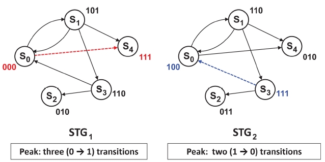
E. Noise Aware FSM State Encoding
Since FSM is a synchronous component controlled by the clock signal of a circuit, it also draws the peak current on the power line (
Huang et al. [33] start from the encoding result produced by the scheme in [34] which targets reducing the total power (i.e., total switching activity) of an input STG. The idea of reducing peak switching among state transi-
tions is to decide whether the value of each bit position in the previously encoded registers is to be complemented or not. For example, if the solution selects to complement bit positions 0 and 3, then all the values in bit positions 0 and 3 in state encoding are complemented. They formulated the problem of determining bit complementing/ uncomplementing into an integer linear programming (ILP), targeted towards minimizing the larger of the maximum numbers of bit positions that switch from 0 to 1 among state transitions and the maximum number of bit positions that switch from 1 to 0.
For
As the process technology scales down, the variation or sensitivity of noise and delay in the clock network becomes worse and worse, which in fact causes a drastic impact on the reliability of the circuit. This paper reviewed several important clock related design problems and the existing techniques that are essential to the highly reliable circuit design. In addition to the introduced design optimization and synthesis issues, there exist other issues that are also important to tolerate or mitigate circuit noise. Those examples are 3D clock design considering through silicon via (TSV) design variation and circuit reliability issues under the power-gated or clock-gated design environment. We hope that this survey helps to find or assess practically useful solutions to the important clock optimization problems that arise in the designs supporting diverse platforms, applications or environments (e.g., [38,39]).

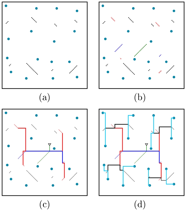
![The flow of the methods of means and medians algorithm [1]. (a) The location of all input clock sinks is fed as input. (b, c) Sinks are equally, using the concept of median of sink locations, partitioned into subregions (arbitrarily in the x- or y-direction) until at most two sinks are left on each subregion. (d) The partitions are merged back in reverse order, using the concept of mean (or center of mass) of the sink locations on the two subregions to be merged to produce an abstract tree topology.](http://oak.go.kr/repository/journal/11750/E1EIKI_2012_v6n4_257_f001.jpg)


![Current waveforms for design s35932. (a) Result of polarity assignment without considering the noise effect by nonleaf nodes in Jang and Kim [15]. (b) Result of polarity assignment with the consideration of the noise effect by non-leaf nodes in Joo and Kim [16].](http://oak.go.kr/repository/journal/11750/E1EIKI_2012_v6n4_257_f005.jpg)

![Structure of adjustable delay buffer [31].](http://oak.go.kr/repository/journal/11750/E1EIKI_2012_v6n4_257_f007.jpg)