In the wafer manufacturing process, humidity is one of the most important environmental factors in a manufacturing factory that must be controlled to maintain the high quality of wafers. An abnormal humidity level can cause a variety of problems such as corrosion, electric failure [1,2], severe adhesion degradation [3,4], and moisture absorption in dielectric materials [5-7].
Conventionally, the importance of the stringent control of the humidity in the photolithography process has been generally emphasized. However, the defect generation problem has never been dealt with before in detail, such as by inspecting defect images with various inspection tools, observing defect trends with the increase of humidity, and identifying the exact defect generation steps and the defect generation mechanism. This paper proceeds to report on all these investigations of the defect generation problem during the photo lithography process including its mechanism.
Organic bottom anti-reflective coating (BARC) has been widely used with the trend towards a miniaturized pattern size for better pattern definition by preventing reflection of photo waves in the photo lithography process. BARC coating is applied using a spin coater at 23℃ followed by curing bake at 230℃ . The defects are generated during the BARC spin coating step.
Abnormally high humidity in an organic BARC coater can cause the generation of defects during the BARC coating stage. Furthermore, the water component in the BARC film behaves as a blocking etching process, resulting in poly pattern bridging and under-etching during the poly etch step.
No other process steps, such as the BARC bake and the PR coating and bake step, are found to create the defects? only the BARC coating step. The contact angles after each of the process steps are evaluated to explain the reason why the defects are generated only in the BARC coating step. The increasing trend in defect generation with the increase of humidity of the BARC coating unit is also analyzed to identify the lower limit that should be stringently controlled to prevent defect generation. The defects were inspected with various inspection tools in blanket wafers and product wafers to identify them exactly using different inspection tools.
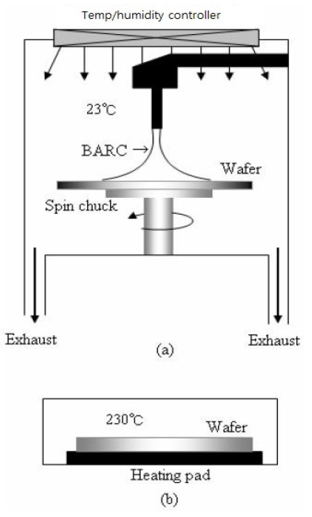
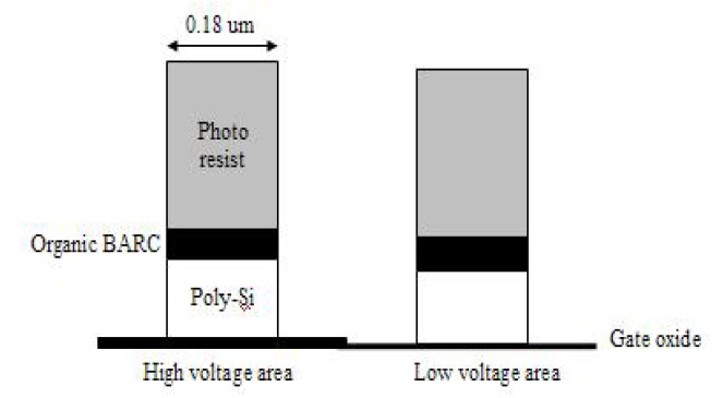
An (100)-oriented p-type wafer with a resistivity of 9?12 Ω-cm was cleaned by 1:19 diluted hydro fluorine and shallow trench isolation was formed. After WELL and threshold voltage adjustment implantation, gate oxide was grown in a conventional furnace at 800℃ with wet oxidation targeting 65 A and 30 A for high and low voltage areas, respectively. Following the gate oxide growth, undoped polysilicon (poly-Si) was deposited at 530℃ with 2,500 A. Photo lithography for the gate patterning was performed with a 0.18 um line width using 248 nm KrF lithography technology after organic BARC (DUV32J; Brewer Science, Rolla, MI, USA) and photoresist (PR) (SR540; Stanford Research Systems, Sunnyvale, CA, USA) coating targeting 750 A and 7,600 A, respectively. A decoupled plasma source (DPS) plasma etching reactor was used for the BARC and poly-Si gate etching process. Fig. 1 shows a detailed process schematic diagram.
The coating step is performed in the following sequence: BARC coating at 23℃ , curing bake at 230℃ , PR coating at 23℃ , and curing bake at 120℃ . After each of the coating and bake steps, the defects are inspected to identify the defect generation step and root cause. No patterned wafer defect inspector (Surfscan6200; KLA-Tencor, Milpitas, CA, USA) was used to inspect the defects in the blanket silicon wafer.
Scanning electron microscopy was used to inspect the defect sites and to find the defect sources. The defect count with the increase of humidity during the BARC coating step was also measured at the product wafers with 0.18 um line width using the patterned wafer defect inspector (AIT, KLA-Tencor) and in the blanket wafer using the Surfscan6200. A microscope and ultraviolet (UV) light projector were also used to find a method for identifying the defects with the different sources. The humidity was controlled by a temperature and humidity controller at the BARC coating unit.
The structure of the BARC coating unit is analyzed to explain why the defects were distributed along the wafer edge. The contact angle for the PR (UV113; Shipley, Marlborough, MA, USA) and organic BARC (DUV30J; Brewer Science) film was measured at different steps to identify the defect generation mechanism using a drop shape analysis system (DSA-100; KRUSS GmbH, Hamburg, Germany).
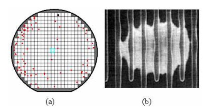
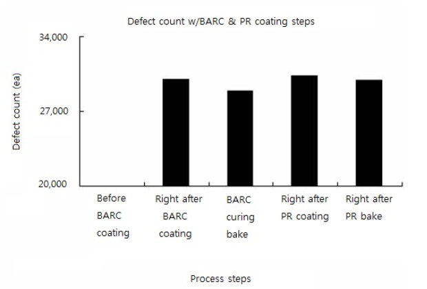
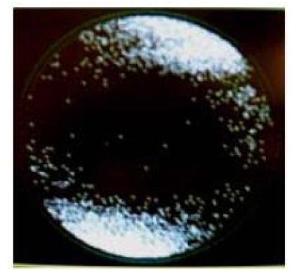
Extreme round-type defects were detected right after the gate photo lithography process, which uses organic BARC (DUV32J), at the wafer edge as shown Fig. 2a. The defects induced extreme pattern bridges in the subsequent BARC etching process as shown in Fig. 2b.
The defect image has a typical shape that can be seen at the viscous source of strong surface tension with the contacted gate patterns as seen Fig. 2b. It can be assumed that the defect is closely related to humidity during the photo lithography process. Evaluation results show the defects are created right after PR coating before the exposure step as shown in Fig. 3. The gate photo lithography process of 0.18 um technology is composed of the following steps: BARC coating at 23℃ , curing bake at 230℃ , PR coating at 23℃ , curing bake at 120℃ , exposure, post exposure bake at 130℃ , development and hard bake at 110℃ .
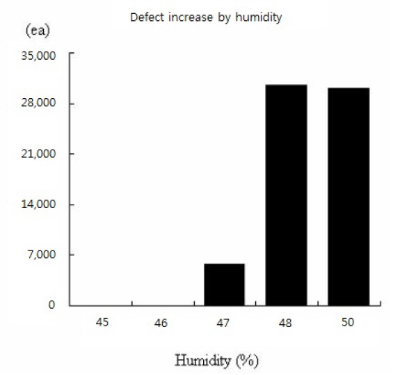
The BARC coating step is found to be the root cause step in which the defects are created as exhibited in Fig. 4.
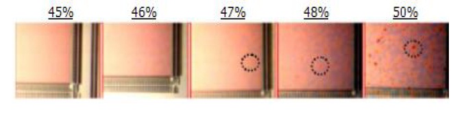
The defect count remains unchanged from the subsequent BARC bake step with no more increase. A drastic defect increase is found beginning at 47% humidity during BARC coating as shown in Figs. 5 and 6 inspected by the Surfscan6200 and microscope, respectively. The results from the blanket wafer and product wafer show exactly the same results.
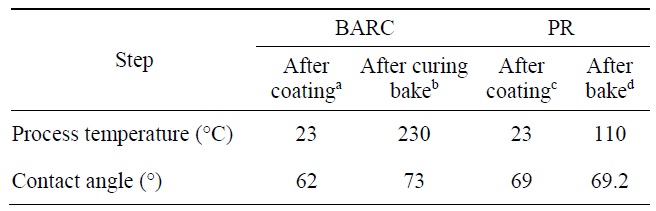
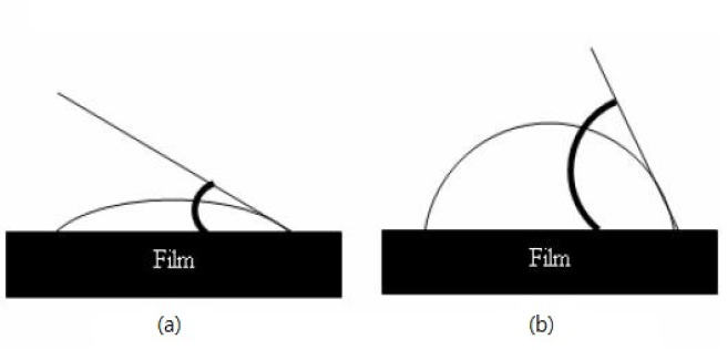
The extreme defect generation right after the BARC coating step can be explained by the hydrophilic property of the BARC film at this step. The narrow contact angle for the BARC film right after coating as shown in Fig. 7 means a more hydrophilic property. The wide contact angle for the subsequent BARC curing bake represented hydrophobicity, resulting in a lack of defect generation, as exhibited in Table 1 and Fig. 4.
The hydrophilic BARC of the narrow contact angle can easily absorb, combine, and react with water creating condensed hydro-organic compounds containing water, whereas hydrophobic BARC after the bake or PR right after coating is unwilling to absorb the water, resulting in no more defect generation. Table 1 and Fig. 4 show that more hydrophilic films generate more defects. A noticeable increase in the contact angle between the coated BARC and baked BARC indicated the hydrophilic property of BARC film before the bake step and hydrophobic property after the bake step through condensation [8]. No difference in contact angle between the coating and bake was found in the case of PR, which is originally a hydrophobic film as explained in Table 1.
[Table 1.] The Contact angles of bottom anti-reflective coating (BARC)

The Contact angles of bottom anti-reflective coating (BARC)
The defects related to the water component act as a blocking material for the etching process, resulting in an extreme poly line pattern bridging by preventing the etching of the BARC film.
The defect map distributed around the wafer edge is estimated to be caused by the exhaust port surrounding the wafer edge in the BARC coating unit as exhibited in Fig. 8. The moisture flows out to the wafer edge by the exhaust pressure directed to the edge of the BARC unit, resulting in higher moisture density around the wafer edge compared to the center area.
Experimental results indicated that during organic BARC coating process the humidity needed to be maintained below 47% to prevent moisture-related defect generation as Fig. 5 clearly shows.
It was found that an extreme defect is created during the BARC coating before the bake, resulting in pattern bridges. Defects are distributed along the wafer edge due to the location of the exhaust port surrounding the wafer edge in the BARC coating unit. The water can thoroughly combine and react with the BARC film with its hydrophilic property right after coating and before the bake. However, the condensed BARC after the bake converts it to a hydrophobic state, which is reluctant to react with water, suppressing the high humidity-induced defect generation. PR is also hydrophobic enough not to react with water even at the high humidity level of 50%, resulting in no high humidity-associated defect generation.
In sum, humidity must be maintained below 47% during the BARC coating process to prevent moisture induced defect generation.