The slow light (SL) in photonic crystal waveguides (PCW) has been receiving interest during the past decade [1-4]. It enhances the light-matter interaction which reduces either the power or the physical length required to observe the same linear and nonlinear effects compared to the fast light regime [5]. In the slow light regime, the optical signal is compressed and hence the pulse amplitude is increased, which causes the enhancement of the linear and nonlinear effects in the structure. Linear effects such as gain, thermo-optic, and electro-optic interactions are scaled with the slow down factor, whereas the nonlinear effects may scale with its square [2, 6].
It is possible to design slow-light structures to modify dis-persion diagrams to obtain high slow down factor and low group velocity dispersion (GVD). These structures have been recently proposed through engineering the geometry of the PCW, chirping the waveguide properties [2, 3], modifying the waveguide width [7], changing the hole size [3], and reshaping the two innermost rows of the holes in W1-PCW[2, 8]. Since disordering limits the accessible group index and bandwidth [3], each method requires high precision fabrication technologies.
Light confinement and dispersion control have been studied in the silicon based slotted PCW in recent years [9-11]. The Electro-Optic (E-O) or nonlinear material injection to the slot region of the slotted PCW results in the light confinement and tuneability of the devices. The field enhancement in an E-O-polymer filled slotted waveguide [10] and the high speed modulation in photonic crystal (PC) Mach-Zehnder geometry have been studied [9, 11]. Also, slow light tuning in slotted PCW has been numerically demonstrated[12]. But the common problem in silicon photonic devices is the temperature dependence of the optical properties due to the thermo-optic effect of silicon [13, 14]. This effect has not been taken into account in the previous research on the slow light structures, whereas it has had a considerable effect on the optical properties of the designed structure. As an example only a 38℃ temperature variation corresponds to variation of 6.8×10⁻³ in refractive index which is enough to perform switching in some PC switches [15, 16]. Therefore, to prohibit undesired change of transmission behaviour of the device caused by temperature variation,accurate temperature control is necessary, thus increasing the size and cost of the devices.
In this paper, we have proposed a potential solution to improve the design of silicon based slow light optical devices. In our silicon based slotted PCW design, we have modified the two innermost rows of the holes. The slot and the two innermost rows are infiltrated with polymer. These modifi-cations change the dispersion of the guided modes in PCW, generate and enhance the slow light over a wideband with very low GVD. However, since the thermal dependence of refractive indices of silicon and polymer are typically opposite, the thermo-optic effect of the polymer can minimize or even eliminate the temperature dependence of the device for a desired operating range. We show that the proposed structure will be stable for temperature variation of up to 60℃. Also the infiltration of the structure can be done after implementation of the main silicon structure, hence the normal fabrication precision is enough to obtain a structure with high group index-bandwidth product.
This paper is organized in four sections. The design of the slow light slotted PCW and the modified structure para-meters to maximize broadband and low group velocity dispersion will be discussed in next section. The design, performance and thermal stability of the proposed structure are studied in section 3. The paper will be concluded in section 4.
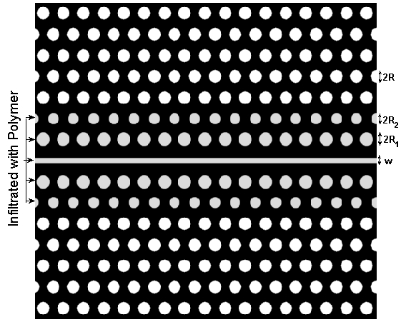
The Planar slotted PCW (SPCW) can be implemented by replacing a row of air holes in the triangular lattice PC with a narrow slot, as displayed in FIG. 1. Since the two innermost rows of holes have the most important impact on the dispersion diagram [1, 8, 17], these two rows are modified. The slot and the two innermost rows are infilt-rated with polymer.
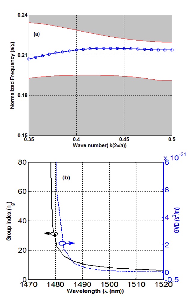
Two dimensional numerical calculations of the band
diagrams are performed by the plane wave expansion method (PWEM) and by selecting an appropriate supercell using the MIT photonic band (MPB) package [18]. Dispersion diagram of the TE mode in the proposed structure is depicted in FIG. 2a, which shows the PBG and single mode range of the structure. Related group index (
are shown in FIG. 2b. The geometry parameters are considered as: silicon refractive index of
birefringent polymers as infiltrating materials. These can be supplied by Chem Optics, Inc. The refractive index of LFR material is about 1.4 at wavelength of 1.55 ㎛ [22, 23].
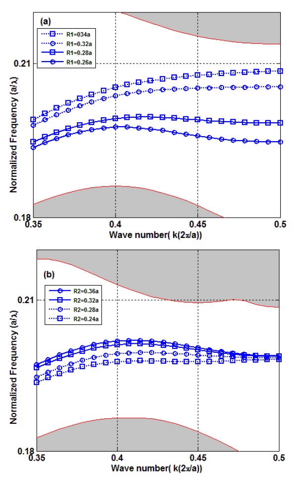
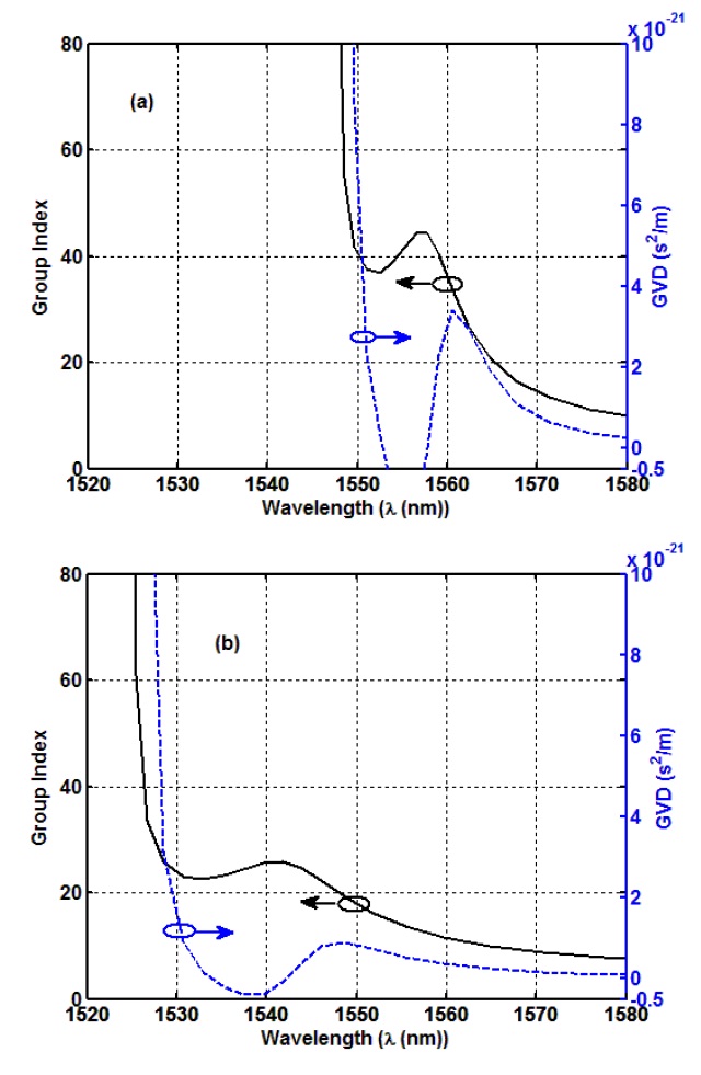
To flatten the dispesion diagram of the fundamental mode in a desired frequency, and to maximize the slow light over a wide bandwidth, the radii of the first and the second innermost rows of the holes are reduced and increased, respectively.
The dependence of the dispersion diagram on the diameter
of the two innermost rows of the holes is illustrated in FIG. 3. The higher R1 will increase the tail of the diagram near band edge (FIG. 3a), whereas the higher R2 will increase the diagram at the middle of the band (FIG. 3b).
Modification of R1 and R2 will affect the available group index and its flatness over a frequency bandwidth. To achieve the slow light with large group index,
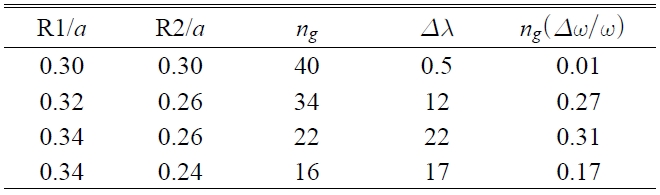
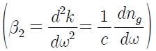
To enable comparison between results, we have calculated the group index-bandwidth products (GBP),
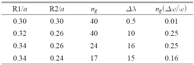
Group index-bandwidth product ng(Δω/ω) of the proposed structure at 25℃ for different radii of two innermost rows of the holes.
Table 1 shows better GBP in comparison with [20] and complies very well with those of [8, 19].
Also, Table 1 shows that a small change in the R1 and R2 values has little effect on the GBP. Therefore the 0.02a ? 8 nm fabrication precision is acceptable.
Temperature dependence of the material refractive index can change the transmission behavior of the optical devices. Meanwhile when the slow light phenomenon is utilized to improve the light-matter interaction, thermo-optic effects will be enhanced [1, 8], hence accurate temperature control must be considered in order to guarantee the stable perfor-mance of the device for a desired temperature range. Krauss
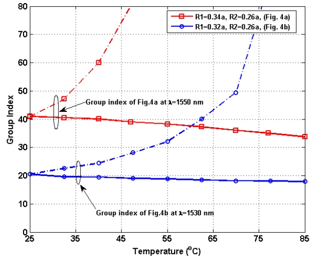
The group index-bandwidth product has been calculated at 85℃ and depicted in Table 2. The comparison of the GBP
in 85℃ and 25℃ (Table. 1 and 2) shows an improvement

Group index-bandwidth product ng(?ω/ω) of the proposed structure at 85℃ for different radii of two innermost rows of the holes.
in GBP while the group index decreases.
A new concept for design of a slow light structure based on silicon photonic crystal wave-guides (PCW) has been introduced. Dispersion engineering of photonic crystal wave-guide is feasible by changing the refractive index of the two innermost rows of the holes in W1 waveguide. Easy fabrication because of no requirement for high precision technology and elimination of thermal dependence of the group index on undesired temperature variation are the main advantages of this structure. The structure parameters were modified to maximize the broadband slow light effect. The accurate design and different sign of the thermo-optic coefficients of the polymer and the silicon make the proposed structure very stable in the range of 60℃ and improve the group index-bandwidth product.