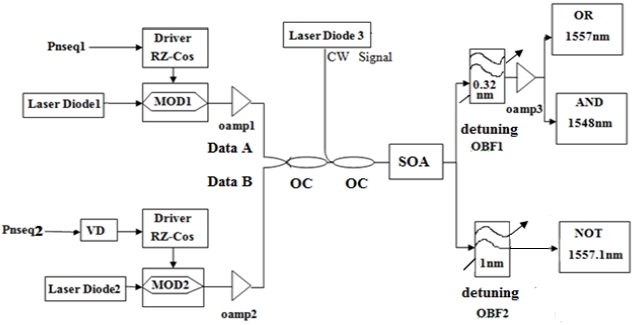
We demonstrate an optical gate architecture using a single SOA to perform
The implementation of node functionalities employing electro-nics can represent the bottleneck in achieving progress toward broadband and flexible optical networks. All-optical processing is especially interested in the high capacity core networks, where optoelectronic conversions should be avoided. The all-optical functions are needed in add-drop and cross-connect fabric such as wavelength conversion, add-drop multi-plexing,clock recovery, regeneration, and simple bit-pattern recognition [1].
Logic gates that operate in the optical domain have been studied for several years due to the prospects of eliminating O-E-O conversions and enabling all-optical networks with above-mentioned applications. There have been many approaches previously reported for realizing optical logic [2-5]. Fre-quency encoding techniques using PPLN waveguides do not have any intensity loss dependent problems but the use of PPLN waveguides makes these implementations temperature and polari-zation sensitive[4]. Proposals based on polarization based logic implementation have some drawbacks as the state of polarization may change at the reflecting or refracting points along the transmission or propagation path[3, 4]. Compared with the nonlinearity of optical fiber, the semiconductor optical amplifier (SOA)-based all-optical signal processing has demonstrated great potential in terms of low power consumption, fast switching time, and optical integration [6-8]. Semiconductor optical amplifier (SOA) is a very attractive non-linear device, but SOA based proposals using interferometric configurations including two or more devices need accurate control and stabilization schemes [9, 10]. Logic gates based on four-wave mixing in SOAs, suffer from low conversion efficiency and polarization dependence [11, 12].
In this work we present simple, reconfigurable and polari-zation independent implementation of all-optical logic operations based on a single semiconductor optical amplifier. We demon-strate the AND, OR NOT logic functions using RZ modulated signals at 40Gb/s. Contrast ratio and extinction ratio values have also been analysed for the different types of logic gates.
The system configuration is depicted in Fig. 1. The wave-lengths of two CW beams generated by Laser Diode1, Laser Diode2 are 1549.3 nm and 1550.7 nm respectively.
Lorentzian laser sources are used as Laser Diode1, Laser
[TABLE 1.] Parameters used in simulation

Parameters used in simulation
Diode2 with FWHM as10MHz and 10dBm power. Pnseq1 and pnseq2 generate pseudorandom binary sequence (PRBS)at high data rate with deterministic polynomial number 1. The data signals (A and B) are modul-ated by two modulators at 40 Gb/s to form return-to-zero (RZ) PRBS signals. The duty cycle of these RZ pulses is 33%. One of the data signals is delayed for several bits so that two data signals with different data patterns are obtained. Both data A and B have the average power of 2 dBm. Optical amplifiers oamp1 and oamp2 are used to amplify data signals.
Laser Diode 3 is generating the probe signal (CW) at 1557.3 nm with FWHM as 10MHz and 0dBm power. The SOA is biased at 200 mA with line width enhancement factor of 6. The standard travelling wave SOA is taken as the amplifier model in our simulation with relevant para-meters as given in Table 1 A tunable Gaussian narrow optical bandpass filter (OBF1) with 0.32 nm bandwidth is used to filter the OR logic and AND logic. Another 1 nm bandwidth gaussian tunable optical bandpass filter (OBF2) is used to filter out the probe signal with NOT output.
In the system two optical bandpass filters with different bandwidths have different functions. In order to get logic OR, the OBF is used to reject the probe carrier and to filter out the sideband component. However, the sideband frequency is very close to that of the probe carrier; so, a narrow optical bandpass filter with 0.32 nm is employed. In the logic AND, the conjugated light has a frequency close to the data signal frequency; so, the OBF is selected with narrow bandwidth. For logic NOT, the OBF required should have a small detuning without suppressing the probe carrier; so, we use the ordinary OBF with 1 nm band-width.Optical amplifier oamp3 is used to amplify AND output power.
The all-optical logic gates are obtained by four wave mixing(FWM), cross gain modul-ation (XGM) and cross-phase modulation in the SOA. Simulation (in Optsim-4.7.1) for output wave form is performed using RZ modulated signals, taking data rate 40 Gb/s using the parameters for the SOA (shown in Table 1). Through properly adjusting the input power levels and the OBF centre wavelength, different logic functions are realized.
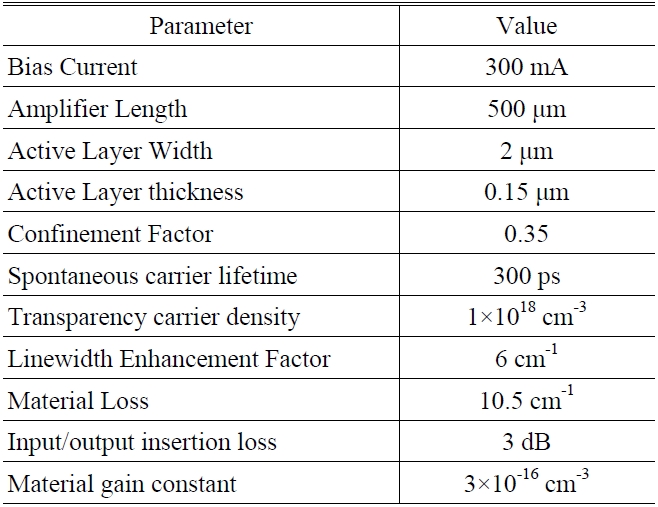
When two modulated, optical return-to-zero (RZ) data signals, combined with a continuous wave probe signal are injected into the SOA, due to cross gain modulation (XGM) and cross phase modulation (XPM) the output optical spectrum of the probe signal becomes broadened. Either data A or B or both launched into the SOA will induce a shifted spectrum. If both the data signals are absent, there will not be any shifted spectrum. OBF with properly large detuning rejects the probe carrier and selects the shifted spectrum. Therefore, the output is logic OR gate.
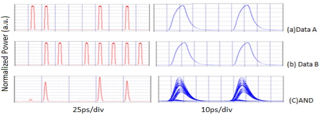
The input data A and B before entering the SOA are shown in Fig. 2(a) and (b), respectively Both the wave-forms have the average of 2.2 dBm. The probe power is 0 dBm. In order to obtain logic OR, the narrow (0.32 nm) OBF1 is employed. OBF1 is detuned -0.3 nm from the probe carrier and the output signal turns to be OR gate, although the pattern effects and amplitude noise appear in the eye diagram [see Fig. 2(c)]. As a penalty, the output signal has a low power level since the OBF1 is detuned far from the probe carrier. Extinction ratio and contrast ratio measured for OR are 18.2 dB and 17 dB respectively.
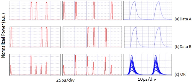
NOT gate operation is obtained due to cross gain modul-ation in semiconductor optical amplifier. When either data A or B are present, the probe signal is gain-modulated with polarity-inverted output, which results in logic NOT output. In order to accelerate the amplitude recovery and remove the pattern effects, OBF2 with small detuning to the probe carrier i.e. -0.2 nm is utilized. As XGM is limited by the gain recovery time of the SOA, the outputs appear to be somewhat saturated in the case of the NOT gate.
Input signal waveform of data A with Laser Diode 2 turned off is shown in Fig. 3(a). Output waveform with good eye diagram can be observed in Fig. 3(b).
When both the data signals are present in the SOA, the conjugated light is generated due to the FWM effect, which
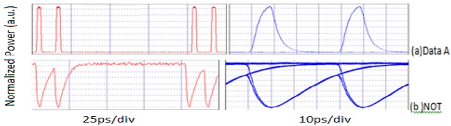
is optically filtered out to implement AND logic. Fig. 4(a) shows the optical spectrum of the probe (CW) signal before
entering into the SOA. Fig. 4(b) shows the spectrum at the SOA output. According to the FWM effect, the conjugated light is generated at 1548 nm and is filtered out by OBF1.
The AND output has a low power level due to the low conversion efficiency of the FWM and is therefore amplified by oamp3.The output signal of logic AND with good eye diagram is shown in Fig. 5(c) for the two data inputs signals 5(a) and 5(b). Maximum extinction ratio and contrast ratio observed for AND logic are 19 dB and 12 dB respectively
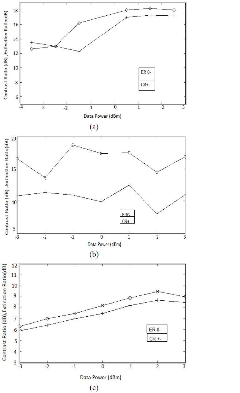
Output eye diagram of the NOT gate is in inverted RZ format, which is also present in practical optical networks. We observe some small residual pulses in the AND gate output where ideally they should not appear. However, this could be improved by optimizing the filter transfer function. The AND output has a low power level due to the low conversion efficiency of the FWM, while the NOT output has a high power level. As the NOT gate is based on XGM effect in the SOA therefore observed extinction ratio is less as compared to those measured for the other gates [13]. We select the output contrast ratio (C.R.) and extinction ratio(ER) as the optimization criteria. For optimum gate performance, C.R. must be as high as possible so that the largest fraction of input exists at the output, E.R. must be as high as possible so that the ‘HIGH’ (1) level can be distinguishable from ‘ZERO’(0). Fig. 6 presents variation of contrast ratio and extinction ratio with variation of the input power of the RZ data signals from -3 to +3 dBm, while at the same time maintaining the CW probe power 0 dBm.The graphs show that maximum E.R is obtained at input data power ~2.2 dBm. Maximum extinction ratio obtained for OR, AND and NOT gates are 18.2 dB, 19 dB and 9.7 dB respectively.
The all-optical scheme for reconfigurable logic operations at 40 GB/s have been proposed.
The logic AND, NOT and OR are obtained by FWM, XGM, and XPM in the single SOA. In our proposed design we achieve the contrast ratio, extinction ratio as 17 dB and 19 dB respectively, which are more adequate for all-optical logic-based information processing. The proposed logic gates have a very simple structure and, as they are based on the semiconductor technology, allow for photonic integration.