The use of a Ti:LiNbO3 symmetric Mach-Zehnder interferometric intensity modulator with a push-pull lumped electrode and a plate-type probe antenna to measure an electric field strength is described. The modulator has a small device size of 46×7×1 mm and operates at a wavelength of 1.3 ㎛. The output characteristic of the interferometer shows the modulation depth of 100% and 75%, and Vπ voltage of 6.6 V, and 6.6 V at the 200 Hz and 1 KHz, respectively. The minimum detectable electric field is ~1.84 V/m, ~3.28 V/m, and ~11.6 V/m, corresponding to a dynamic range of about ~22 dB, ~17 dB, and ~6 dB at frequencies of 500 KHz, 1 MHz and 5 MHz, respectively.
Electric field sensors are widely used in the electromagnetic compatibility (EMC) technology area and their importance is growing with the progress of the mobile multimedia communi-cation fields [1]. To evaluate the EMC it is necessary to accurately evaluate the strength and distribution of electromagnetic field surrounding the electronic equipment. Even though various kinds of sensors have been developed, all-optical electric-field sensors have several unique advantages [2-5]. Some of their benefits over electrical devices used in the measurement of electric fields are:
The sensor provides improved measurement accuracy by reducing susceptibility to electrical noise because the sensor is made of dielectric materials.
The sensor provides a non-contact measurement of electric field.
The sensor may be placed in hostile or remote areas because optical fibers are capable of transmitting signals with high fidelity in noisy environments and over long distances.
The sensor is electrically isolated, thus providing operator instrument safety.
The sensor is small enough to be used where space is a constraint.
Because the electric field sensor is an all-optical and an all-dielectric device, it offers minimal disturbance to the electric field to be measured. It also operates without a battery, so measurements can be conducted over a long period. Its sensing part does not contain any electronic devices or circuits, so it can easily be miniaturized.
The sensor system uses a laser whose output is provided as input to the photonic electric field sensor which is placed in the EM environment. The optical output of the sensor is modulated by the electric field present in the EM environ-ment.The optical output which is a linear representation of the electric field present in the EM environment is provided to the optical fiber. The output optical fiber is connected to a detection system consisting of an optical photo-detector, low-noise preamplifier, and rf spectrum analyzer.
Hybrid electro-optical electric-field sensors using a coplanar waveguide antenna [2], a circular antenna fabricated on mica sheet [3], and Mach-Zehnder modulators utilizing traveling-wave electrode structures on the LiNbO3 substrate were reported previously. The present paper presents an electro-optical Mach-Zehnder modulator-type electric-field sensor with push-pull lumped electrode structures and plate-type probe antennas. To measure the relative low frequency electric field strength, a probe antenna of wide effective area is more useful than the usual dipole antenna. First, we describe the configuration and theory of the new sensor. Then the electrical and optical properties of the sensing part are presented. Finally, the sensing experimental system, measurement results, and discussion are given.
II. THEORY, FABRICATION AND PROPERTIES OF Ti:LiNbO3 MACH-ZEHNDER INTERFEROMETRIC MODULATOR
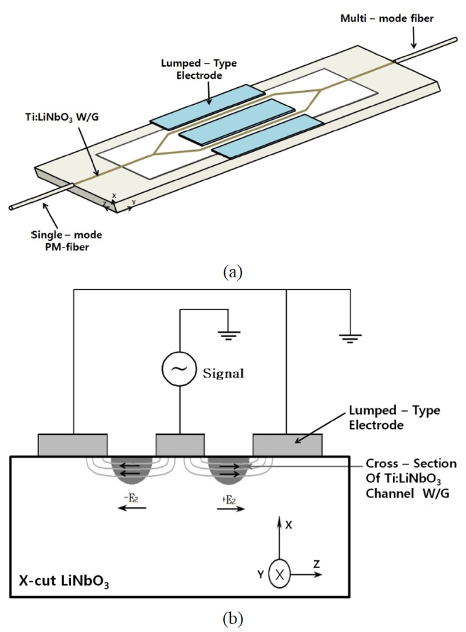
A configuration of the electro-optic sensing part is shown in Fig. 1(a). The optical waveguide circuit is a symmetric Ti:LiNbO3 Mach-Zehnder interferometer with lumped-type push-pull electrode structure.[6-7] The device has 3 dB input splitter and output combiner. Light input to the device is received from a polarization maintaining singe mode fiber
and output from the device is connected to a multimode fiber. The applied voltage (namely, electric field) produces equal and opposite phase shifts in the light beam propagating in the two parallel channel waveguides (namely, arms), thereby leading to a net phase shift of twice the phase shift for each channel. When the two light beams recombine at the output combiner the phase modulation is converted to an amplitude-modulated signal at the same frequency of the applied signal voltage. Therefore the light signal amplitude is proportional to the applied electric field.
In the electrode structure on the device shown in Fig. 1(b), the applied signal voltage produces the electric field along the Z-axis direction, Ez which cross the channel waveguides in the lithium niobate. This Z-directed electric field interacts with the light beam propagating in the channel waveguide to produce electro-optic modulation. The electric field vector of the light wave propagating in the Ti:LiNbO3 channel waveguide should also be oriented in the Z-direction(namely, along the optical axis). This mode is referred to as the Transverse Electric (TE) mode (which is also called the extraordinary mode). This electric field generated by the applied voltage modifies the extraordinary refractive index, ne of the substrate through the linear electro-optic effect which is given by

where r33 is the electro-optic coefficient of lithium niobate (~30 pm/V) and Γ(0< Γ< 1) accounts for the numerical degree of the mutual interaction between the applied electric field and the optical field in the channel wave-guides[8]. The corresponding phase change in the light beam propagating in each arm is given by

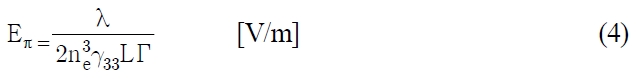
where λ is the wavelength of the light and L is the electrode length. The electrodes are oriented such that the electric field through each arm has opposite polarity and therefore the two phase changes add in determining the net phase difference when the optical signals recombine at the output. In terms of the applied voltage V and the electrode gap g the total phase change at the output combiner is as follows:
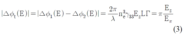
where the half wave field Eπ is defined by
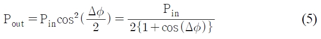
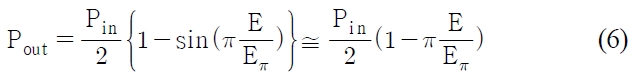
The phase shift produced by the electric field in each arm is converted to amplitude intensity modulation at the combiner of the interferometer. The optical power transfer function of the device can be expressed as follows:
where
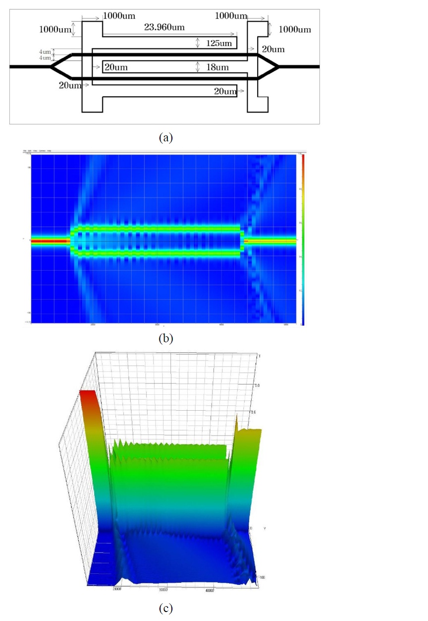
The single-mode channel waveguide symmetric interfero-meters with lumped electrodes were designed for operation at ~1.3 ㎛ in an X-cut, Y-propagating LiNbO3 substrate (46×7×1 mm) as shown in Fig. 2(a). The interferometer had a 7.5 ㎛ channel width, total branching angle of 1.2°, 25 mm straight arm length, and arm separation of 26 ㎛. The BPM-CAD simulation results of light wave propagation for the interferometer are shown in Fig. 2(b), (c) [9]. It is clearly seen that incident light splits and combines almost equally at the input and out Y-branch, respectively. The dimension and arrangement of the lumped electrode structure is also shown in Fig. 2(a).
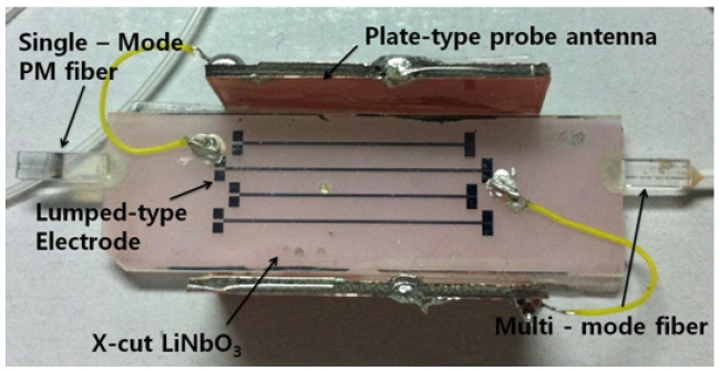
The Mach-Zehnder interferometer modulators were fabricated on X-cut LiNbO3 substrates using standard photolithographic technique. Channel waveguides were formed by diffusing a 1050 A-thick, 7.5 ㎛-wide stripe of Ti film at 1050℃ in wet ambient. The substrate edges were optically polished to allow butt coupling and pig-tailing. ~3500 A-thick SiO2 buffer layer was deposited using e-beam evaporation and 99.99%pure SiO2 pellets to prevent the propagation loss caused by the optical absorption of the electrode metal.~3500 A-thick aluminum lumped electrodes were fabricated to allow the sensing of electric field. Polarization maintaining single-mode and multi-mode optical fibers were attached to the input and output waveguides, respectively. Finally, a 20 × 10 mm plate-type external probe antenna of copper was attached to the electrode on the substrate. Figure 3 is the microscope surface photograph of the fabricated device with attached optical fibers and a copper plate-type antenna.
2.3. Performance Evaluations of Interferometers
We first tested the devices without attached fibers at
low frequencies (200 Hz and 1 KHz). Performance characteri-zation was carried out at 1.3 ㎛ wavelength by butt coupling from a pigtailed tunable laser. TE polarized light from the pigtailed tunable laser was butt coupled into the devices and collected at the output by a microscope objective and focused onto a photo-detector for characterizations. TE or TM input polarization was selected by proper adjustment of a fiber polarization controller. Single-mode propagation for TE polarization was observed in the interferometers.
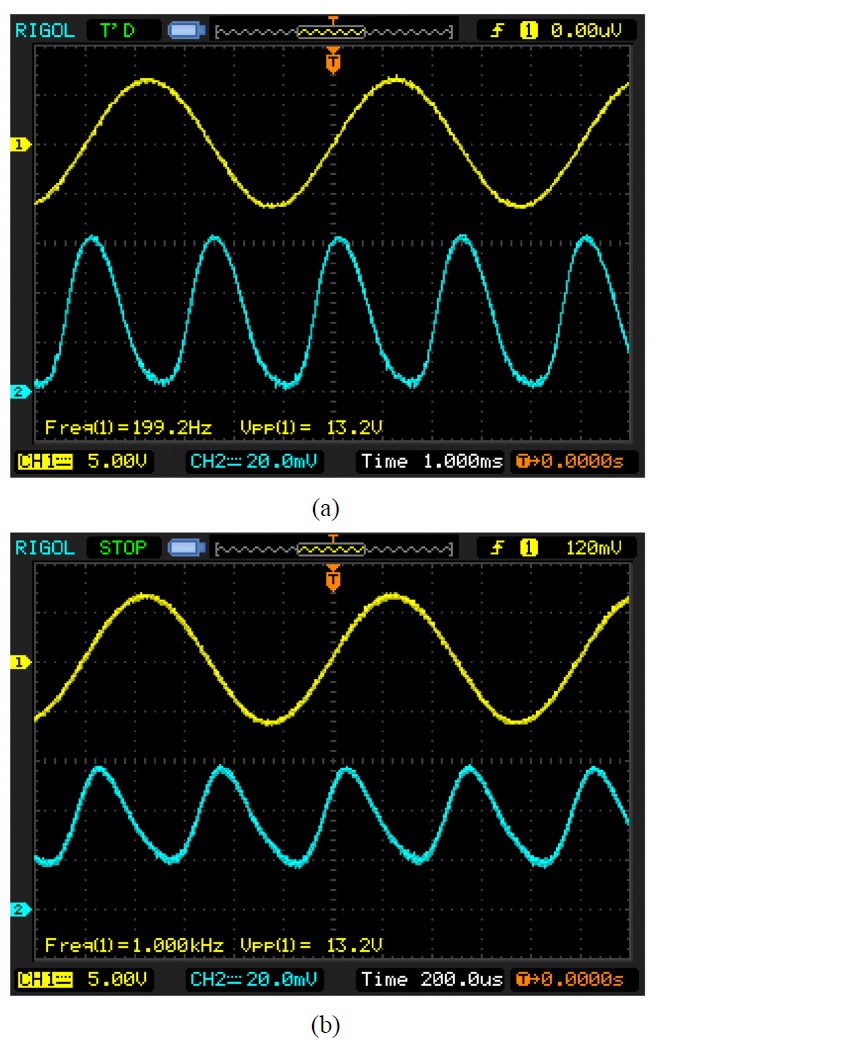
The modulation depth and the half-wave voltage Vπ were measured by applying a sinusoidal voltage signal large enough to drive the device output between maximum and minimum. Figure 4 shows oscilloscope traces of a 200 Hz and 1 KHz sinusoidal voltage drive signal and the response as measured by the photo-detector. The device has a 25 mm electrode length and a 15.5 ㎛ gap. It exhibited the modulation depths of 100% and 75%, and Vπ voltage of 6.6 V and 6.6 V at modulation frequencies 200 Hz and 1 KHz, respectively. The overlap integral Γ deduced from Fig.
4 is about 0.2, which is lower than we expected. The reason for low overlap integral is that the electrode arrangement along channel arms was not optimized. As the frequency of applied electrical signal increases it was observed that the modulation depth decreased as shown in Fig. 4. The reason for this change is not clear although possibilities include imperfect conductive contacts to the device electrodes due to probe contact, non-uniform electrode thickness, and field fringing effects due to the electrode geometry.
III. MEASUREMENT AND EXPERIMEMTAL RESULTS
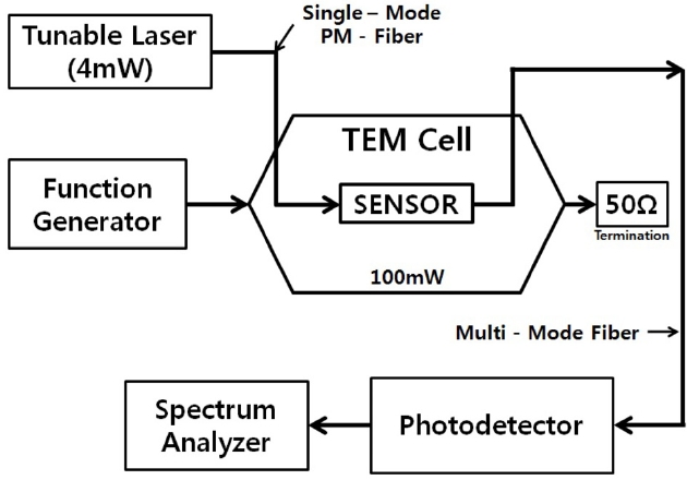
Frequency tests, evaluating the minimum detectable field and frequency response of the fiber coupled sensor were performed using a tunable laser operating at a wavelength of 1.3 ㎛. Incident optical power was of the order of ~14 mW. Figure 5 shows a block diagram of the experimental setup. The device was tested in a uniform electric field by placing it in a TEM cell (TescomTC-5010A) as indicated in Fig. 5. The optical fibers are fed through the sloping walls of the TEM cell and connected to the laser and the photo-detector via FC/PC fiber optic connectors. The 20 ~ -20 dBm (100 mW~10 μW) RF input to the TEM cell corresponds to the electric field strength from 0.293 V/m to 23.2 V/m. The actual field intensity experienced on the sensor substrate is 0.66 V/m due to the high dielectric constant of LiNbO3 (ε?35).[7]The RF power travels through the TEM cell in the same direction as the propagation of light in the optical fibers and the sensor.
3.2. Test Results and Discussions
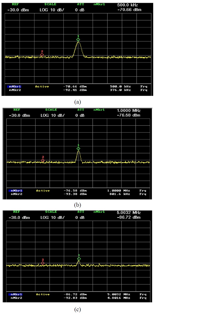
Fig. 6 shows the spectrum analyzer outputs for a 20 dBm input to the TEM cell at frequencies of 500 KHz, 1 MHz, and 5 MHz. The measured rf powers received at the
photo-detector were measured to -70.66 dBm, -76.58 dBm, -86.72 dBm at the applied rf frequencies, respectively. Therefore, the frequency response of the sensor was obtained in the TEM cell as shown in Fig. 7. The 0.66 V/m field across the sensor would cause a peak phase difference of
~17 dB, and ~6 dB, respectively at the frequencies. The minimum detectable electric field is~1.84 V/m, ~3.28 V/m, and ~11.6 V/m based on the Emin = 23.2 × 10(-SNR/20).
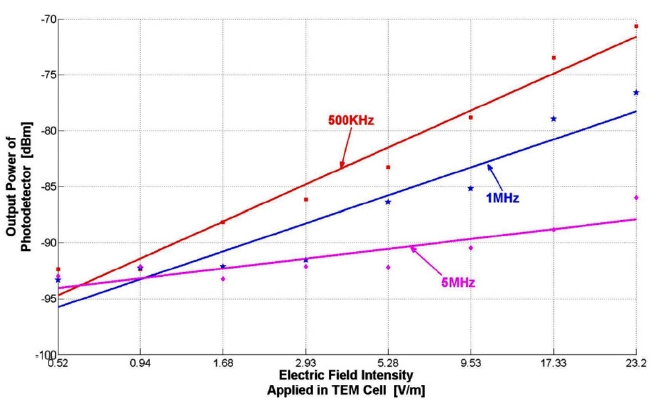
Figure 8 shows the sensitivity curves at frequencies of 500 KHz, 1 MHz, and 5 MHz. As shown in Fig. 8, the sensor exhibits a linear-like response tendency for the applied electric field intensity from 0.293 V/m to 23.2 V/m, corresponding to a dynamic range of about ~22 dB, ~17 dB, and ~6 dB at frequencies of 500 KHz, 1 MHz and 5 MHz, respectively.
We have fabricated an electric field sensor which integrated Ti:LiNbO3 Mach-Zehnder interferometer and conventional lumped push-pull electrodes with a plate-type probe antenna, which utilizes the electro-optic effect to modulate the phase of the light propagating in each arm of the device. The sensor has a small device size of 46×7×1 mm and operates at a wavelength of 1.3 ㎛. The output characteristic of the interferometer shows the modulation depth of 100% and 75%, and Vπ voltage of 6.6 V and 6.6 V at the 200 Hz and 1 KHz, respectively. The minimum detectable electric field is ~1.84 V/m, ~3.28 V/m, and ~11.6 V/m at the fre-quencies 500 KHz, 1 MHz, and 5 MHz, respectively. The sensor exhibits linear-like response tendency for the applied electric field intensity from 0.293 V/m to 23.2 V/m, corresponding to a dynamic range of about ~22 dB, ~17 dB, and ~6dB at frequencies of 500 KHz, 1 MHz and 5 MHz, respectively.
For the future, we will try to improve the sensitivity, response speed, and detectable frequency range. To realize high sensitivity, it is necessary to improve the efficiency of the optical modulator itself and to reduce the noise of the optical detector as well as that of light source. Because sensitivity of an electric field sensor using a Ti:LiNbO3 optical modulator is strongly affected by the shape of a electrode we will apply various antenna electrode structures such as dipole antenna, loop antenna, and segmented patch antenna into symmetric and asymmetric Mach-Zehnder inter-ferometers.