검색 전체 메뉴
PDF
맨 위로
OA 학술지
Optimal Design of Dielectric-Filled Plasmonic Slot Waveguide with Genetic Algorithm
  • 비영리 CC BY-NC
  • 비영리 CC BY-NC
ABSTRACT
Optimal Design of Dielectric-Filled Plasmonic Slot Waveguide with Genetic Algorithm
KEYWORD
Surface plasmon polariton , Waveguide , Genetic algorithm
  • I. INTRODUCTION

    Plasmonic waveguides have been considered promising candidates to guide light beyond the diffraction limit by using a surface plasmon-polariton that propagates along the interface between a metal and a dielectric medium [1]. Various types of plasmonic waveguiding structures have been proposed, such as insulator-metal-insulator (IMI) [2, 3], metal-insulator-metal (MIM) waveguides [4-6], metallic nanowires [7], and metallic nanoparticle arrays [8].

    However, the tight confinement of propagating light power in plasmonic waveguides is fundamentally associated with high ohmic loss in the metal, and so plasmonic waveguides have an intrinsic trade-off between field confinement (mode size) and propagation loss. To overcome this problem, several different waveguides have been suggested [9-15]. Feng et al. reported that a partial dielectric-filled slot waveguide improves the field localization while keeping the propagation loss low [16]. However, their design procedure for improving the propagation characteristics was sequential and therefore non-optimal design parameters may have been selected.

    In this paper, we focus on the dielectric-filled slot plasmonic waveguide and theoretically investigate the propagation characteri-stics at the telecom wavelength of 1550 nm. The mode field and its propagation characteristics were obtained by use of the finite element method (FEM). We first examine the effective index and propagation length for different geometries. The symmetric geometries are employed here for efficient coupling with other photonic structures. We present a systematic design procedure that is applicable to the shape optimization of a dielectric-filled slot waveguide using the genetic algorithm (GA). We obtain a plasmonic waveguide that has high confinement and a moderate pro-pagation length with optimal propagation characteristics.

    II. PROPAGATION CHARACTERISTICS OF DIELECTRIC-FILLED PLASMONIC SLOT WAVEGUIDES

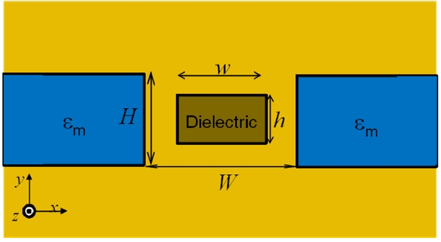
    Figure 1 shows a schematic diagram of the dielectric-filled plasmonic slot waveguide. The structure consists of a symmetric plasmonic slot waveguide with a dielectric core in the slot between metals surrounded by an infinite homo-geneous dielectric cladding. The slot has a width W and thickness H, and the dielectric core has a width w and thickness h. In this paper, Ag is chosen as the metal, silicon as the dielectric core, and silica (SiO2) as the cladding. The corresponding dielectric constants are ε m= -86.6424 + 8.7422i, ε d=12.25, and ε c=2.13[17] at 1550 nm. The characteristics of propagation modes supported by this geometry have been investigated in detail using the FEM.

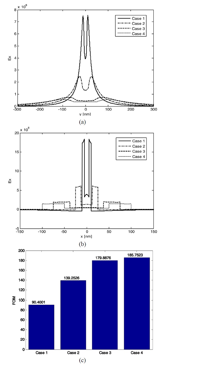
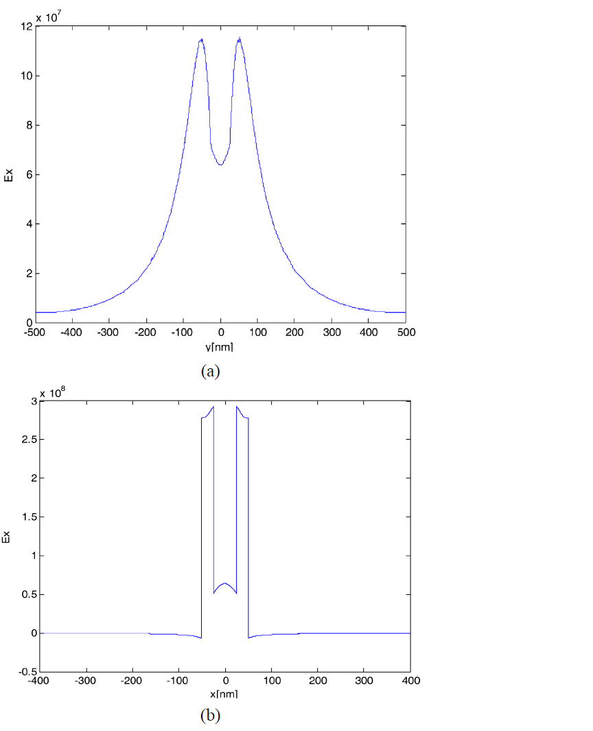
    Fig. 2(a) and 2(b) show the field distributions of the dominant electric field component, for a dielectric core of w=50 nm and h=50 nm and a slot of W=100 nm and H=100 nm, along the center of the core dielectric vertically

    and horizontally, respectively. In the dielectric-filled plasmonic slot waveguide, the electric field is focused between the metal and the dielectric core owing to the charge distribution

    on the edge of both metal regions. This geometry thus operates like a capacitor with a dielectric filling in that the electric field has a dominant component in the x direction (ratio of the peak values Ex/Ey=58.8 vertically and 931.6 horizontally in this model).

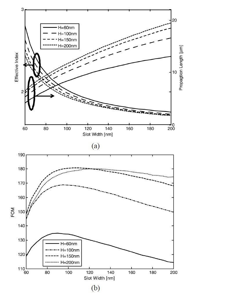
    In Fig. 3(a) we show the effective index neff and the propagation length Lsp (defined by the 1/e field length) of the propagating mode of the dielectric-filled plasmonic slot waveguide as a function of the slot width W for different slot thicknesses at a fixed dielectric core size of w=50 nm and h=50 nm. We can note that the effective index of the mode decreases at a fixed dielectric core size as the slot width W increases because the electric field produced by the electric charge on the metal at the interface between the slot and the metal becomes weak, and therefore the velocity of the mode increases. It is also found that the propagation length increases as the slot width W increases. As the slot width decreases, the fraction of modal power in the metal at the interfaces increases, resulting in a decreasing propagation length.

    In Fig. 3(b) we show the figure of merit (FOM) of the propagating mode of the slot plasmonic waveguide as a function of the slot width W for different slot thicknesses at a fixed dielectric core size, similarly to that in Fig. 3(a). The FOM is defined here as

    image

    where A is taken as the area inside which half of the mode power is distri-buted and α is the imaginary part of the complex pro-pagation constant β /k0 with k0 the free-space propagation constant [18]. Unlike the effective index, the FOM has no monotonic behavior because as slot width increases, the propagation length increases but mode size also increases at a different rate, resulting in the FOM having a maximum. In order to obtain optimal propagation characteristics, the design procedure for optimal propagation characteristics, therefore, should be not sequential but rather a systematic and simultaneous one where all the variables affecting the FOM are varied at the same time.

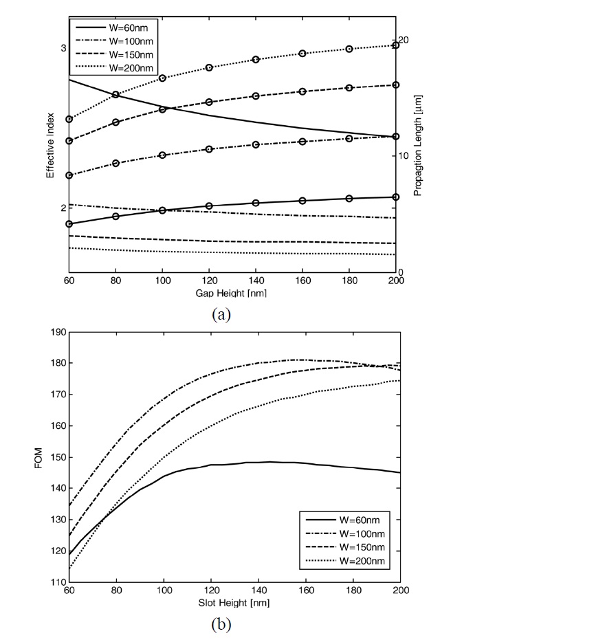
    In Fig. 4(a) we show the effective index neff and pro-pagation length Lsp of the propagating mode of the slot

    plasmonic waveguide as a function of the slot thickness H for different slot widths W at a fixed dielectric core size of w=50 nm and h=50 nm. We observe that as the slot thickness H increases, the effective index decreases and the propagation length increases as in Fig. 3(a).

    In Fig. 4(b) we show the FOM of the propagating mode of the slot plasmonic waveguide as a function of the slot

    thickness H for different slot widths at a fixed dielectric core size, similarly to that in Fig. 4(a). We note that although it is less sharp, the trend is still non-monotonic with the slot thickness H.

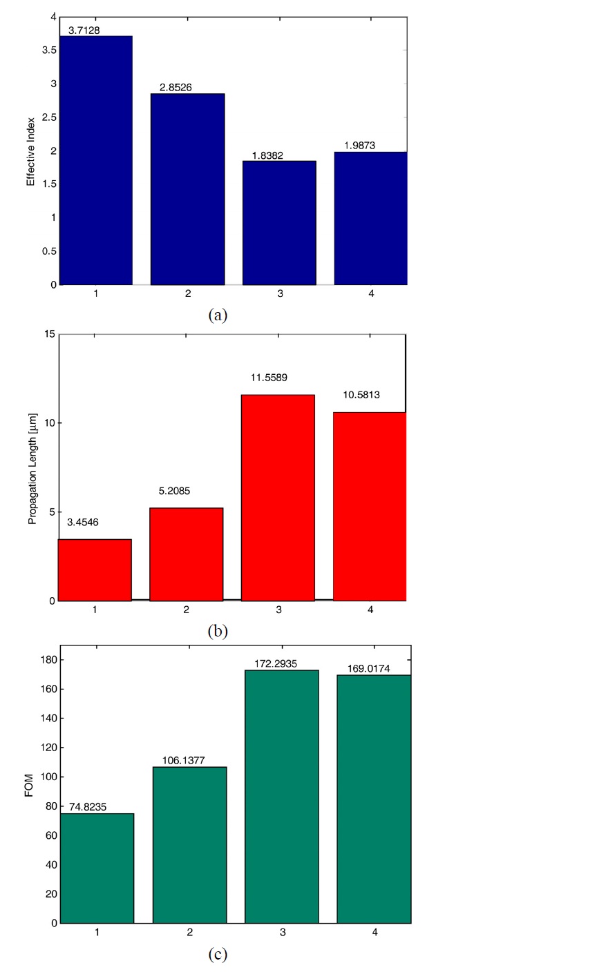
    To further investigate the effect of the dielectric core and the slot on the propagation characteristics, we need to analyze the effective index, propagation length, and FOM for different dielectric-filled plasmonic slot waveguides. The structures we studied here are characterized by the following parameters: a common metal slot of width and thickness W=100 nm and H=100 nm, with case 1 (w, h) = (100 nm, 100 nm) (simple slot waveguide), case 2 (100 nm, 50 nm), case 3 (20 nm, 20 nm), and case 4 (50 nm, 50 nm). In Fig. 5(a), (b), and (c), we show the effective index neff, propagation length Lsp and FOM of the pro-pagating mode of the slot plasmonic waveguides. The mode field of case 3 becomes less localized between the slot and the core (inferred from the lower effective index) but it has a long propagation length, and the FOM of case 3 is found to be the maximum among the four analyzed geometries. It is evident from these results that dielectric-filled plasmonic slot waveguides may have higher FOM than simple plasmonic slot waveguides.

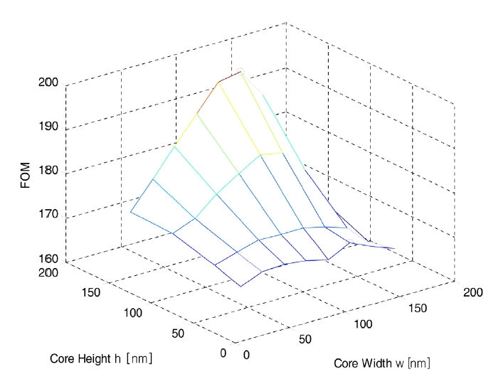
    We have explored further different geometries with square slots and dielectric cores since we obtained the maximum FOM for case 3, which was a geometry with a square slot and core. The geometrical values analyzed here are as follows: W=H (square slot) and w=h (square dielectric core), with case 1 (W,w)=(20 nm, 10 nm), case 2 (50 nm, 25 nm), case 3 (150 nm, 75 nm), and case 4 (200 nm, 100 nm). Fig. 6(a), (b) and (c) show the lateral and horizontal distri-butions of the dominant electric field component along the line passing through the center of the dielectric core and the FOM. The field distributions remain essentially unchanged in that the dominant electric field is maximized at the edge of the core and most of the power is distributed between the metal and the core.

    III. OPTIMAL DESIGN

    For this optimization problem, sequential quadratic pro-gramming (SQP), a nonlinear programming technique which is iterative and uses the gradients of the objective and constraint functions, was used. [19]. One of the disadvantages of using SQP and other approaches based on gradient information is that it is not known whether the final solution denotes the global optimum or simply a local optimum unless the objective function is convex in design parameter space. In Fig. 7, we show the variation of the FOM with the height h and width w of the dielectric core with the thickness H and width W of the metal slot fixed at 200 nm. Since we focus on the dielectric-filled plasmonic slot waveguide in this paper, we know that the optimal values here are local optima, which is usual with techniques using gradient information. The result confirms the fact that it is not possible to find the global optimum by using only the designers’ intuition or experience due to the complexity of

    the objective function. In the present case, in order to search for the global maximum, we employ a genetic algorithm [20-21].

    To design the shapes of the dielectric core and metal slot in the dielectric-filled slot waveguide, we take the objective function as the FOM defined earlier, which combines the performances of field confinement and long propagation length and uses them to determine the optimal parameters.

    We solve the following optimization problem:

    Maximize FOM(x)

    image

    where x is a 4-dimensional design variable vector whose components denote the height h and width w of the core, and the thickness H and width W of the metal slot,respectively. The values

    image

    denote the lower and upper bounds of each design variable, respectively. The condition of is employed to meet the shape requirement that the dielectric is to be inserted into the metal slot. The lower and upper search bounds of the design parameters are 10 nm and 200 nm, respectively.

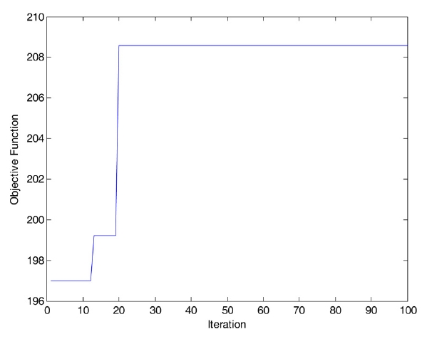
    In the genetic algorithm, the initial population is created randomly. Crossover and mutation are performed based on random numbers. As a result, the genetic algorithm performs differently for each run under the same analysis conditions. Optimization using the GA is performed 100 times, each with a population size of 10, with a crossover rate of 0.2, and hence the mutation rate was 0.8. In Fig. 8, we show how the genetic algorithm optimizes the objective function as generations proceed. The optimal parameters are h =194.5 nm, w = 112.4 nm, H = 198.3 nm, and W = 196.7 nm and its corresponding FOM is 208.6.

    IV. CONCLUSIONS

    We investigate the propagation characteristics of the dielectric-filled plasmonic slot waveguide. We employ the FEM and examine the effect of the slot dimensions on propagation characteristics such as the effective refractive index, propagation length, and a FOM combining both confinement and loss effects. The field distributions of the propagation mode for the slot waveguide were investigated numerically in detail. Furthermore, we carried out optimization of the waveguide slot for high mode confinement and a long propagation length, between which there is an intrinsic tradeoff with the design parameters including the width and height of the core and the width and thickness of the metal slot. We made a comparison between SQP and GA approaches and found that GA is an efficient and powerful approach to the optimization since it is not known whether the final solution denotes the global optimum or merely a local optimum unless the objective function is convex in design parameter space. The approach proposed here was found to be useful and applicable to designing highly integrated nanometric optical circuits.

참고문헌
  • 1. Barnes W. L, Dereux A, Ebbesen T. W (2003) “Surface plasmon subwavelength optics” [Nature] Vol.424 P.824-830 google cross ref
  • 2. Berini P (2006) “Figures of merit for surface plasmon waveguides” [Opt. Express] Vol.14 P.13030-13042 google cross ref
  • 3. Bozhevolnyi S. I, Volkov V. S, Devaux E, Laluet J. Y, Ebbesen T. W (2006) “Channel plasmon subwavelength wave-guide components including interferometers and ring resonators” [Nature] Vol.440 P.508-511 google cross ref
  • 4. Selker R, Selker M. D, Catrysse P. B, Brongersma M. L (2004) “Geometries and materials for subwavelength surface plasmon modes” [J. Opt. Soc. Am. A] Vol.21 P.2442-2446 google cross ref
  • 5. Berini P (2008) “Bulk and surface sensitivities of surface plasmon waveguides” [New J. Phys.] Vol.10 P.105010 google cross ref
  • 6. Park J, Kim H, Lee B (2008) “High order plasmonic Bragg reflection in the metal-insulator-metal waveguide Bragg grating” [Opt. Express] Vol.16 P.413-425 google cross ref
  • 7. Krenn J. R, Lamprecht B, Ditlbacher H, Schider G, Salerno M, Leitner A, Aussenegg F. R (2002) “Nondiffraction-limited light transport by gold nanowires” [Europhys. Lett.] Vol.60 P.663-669 google cross ref
  • 8. Maier S. A, Kik P. G, Atwater H. A, Meltzer S, Harel E, Koel B. E, Requicha A. A. G (2003) “Local detection of electromagnetic energy transport below the diffraction limit in metal nanoparticle plasmon waveguides” [Nat. Mater.] Vol.2 P.229-232 google cross ref
  • 9. Holmgaard T, Bozhevolnyi S. I (2007) “Theoretical analysis of dielectric-loaded surface plasmon-polariton waveguides” [Phys. Rev. B] Vol.75 P.245405 google cross ref
  • 10. Degiron A, Dellagiacoma C, McIlhargey J. G, Shvets G, Martin O. J. F, Smith D. R (2007) “Simulations of hybrid long-range plasmon modes with application to 90° bends” [Opt. Lett.] Vol.32 P.2354-2356 google cross ref
  • 11. Berini P (2007) “Air gaps in metal stripe waveguides supporting long-range surface plasmon polaritons” [J. Appl. Phys.] Vol.102 P.033112 google cross ref
  • 12. Guo J. P, Adato R (2006) “Extended long range plasmon waves in finite thickness metal film and layered dielectric materials” [Opt. Express] Vol.14 P.12409-12418 google cross ref
  • 13. Guo J. P, R Adato (2008) “Control of 2D plasmon-polariton mode with dielectric nanolayers” [Opt. Express] Vol.16 P.1232-1237 google cross ref
  • 14. Oulton R. F, Sorger V. J, Genov D. A, Pile D. F. P, Zhang X (2008) “A hybrid plasmonic waveguide for subwave-length confinement and long-range propagation” [Nat. Photonics] Vol.2 P.496-500 google cross ref
  • 15. Salvador R, Martinez A, Garcia-Meca C, Ortuno R, Marti J (2008) “Analysis of hybrid dielectric plasmonic wave-guides” [IEEE J. Select. Topics Quantum Electron.] Vol.14 P.1496-1501 google cross ref
  • 16. Feng N. N, Brongersma M. L, Negro L. D (2007) “Metal-dielectric slot-waveguide structures for the propagation of surface plasmon polaritons at 1.55 ㎛” [IEEE J. Quantum Electron.] Vol.43 P.479-485 google cross ref
  • 17. Palik E 1985 Handbook of Optical Constants of Solids google
  • 18. Buckley R, Berini P (2007) “Figures of merit for 2D surface plasmon waveguides and application to metal stripes” [Opt. Express] Vol.15 P.12174-12182 google cross ref
  • 19. Hosseini A, Nieuwoudt A, Massoud Y (2007) “Optimizing dielectric strips over a metallic substrate for subwavelength light confinement” [IEEE Photon. Technol. Lett.] Vol.19 P.522-524 google cross ref
  • 20. Michalewicz Z 1996 Genetic Algorithms + Data Structures = Evolution Programs google
  • 21. Lee K, Jung J (2011) “Design of plasmonic slot waveguide with high localization and long propagation length” [J. Opt. Soc. Korea] Vol.15 P.305-309 google cross ref
이미지 / 테이블
  • [ FIG. 1. ]  Schematic diagram of a dielectric-filled plasmonic slot waveguide.
    Schematic diagram of a dielectric-filled plasmonic slot waveguide.
  • [ FIG. 2. ]  (a) The vertical field distribution of the dominant electric field component and (b) the lateral distribution of the dominant electric field component along the center of the dielectric core for a dielectric core of w=50 nm and h=50 nm and a slot of W=100 nm and H=100.
    (a) The vertical field distribution of the dominant electric field component and (b) the lateral distribution of the dominant electric field component along the center of the dielectric core for a dielectric core of w=50 nm and h=50 nm and a slot of W=100 nm and H=100.
  • [ FIG. 3. ]  (a) The effective index and propagation length and (b) the FOM of the propagation mode of the dielectric-filled plasmonic slot waveguide as a function of the slot width W for different slot thicknesses at a fixed dielectric core size of w=50 nm and h=50 nm.
    (a) The effective index and propagation length and (b) the FOM of the propagation mode of the dielectric-filled plasmonic slot waveguide as a function of the slot width W for different slot thicknesses at a fixed dielectric core size of w=50 nm and h=50 nm.
  • [ FIG. 4. ]  (a) The effective index and propagation length (The solid line denotes the effective index and the symbols plus non-solid line the propagation length.) and (b) FOM of the propagation mode of the dielectric-filled plasmonic slot waveguide as a function of the slot width W for different slot thicknesses at a fixed dielectric core size of w=50 nm and h=50 nm.
    (a) The effective index and propagation length (The solid line denotes the effective index and the symbols plus non-solid line the propagation length.) and (b) FOM of the propagation mode of the dielectric-filled plasmonic slot waveguide as a function of the slot width W for different slot thicknesses at a fixed dielectric core size of w=50 nm and h=50 nm.
  • [ FIG. 5. ]  (a) The effective index (b) propagation length and (c) FOM for several dielectric-filled plasmonic slot waveguides:W=100 nm and H=100 nm with case 1 (wh)=(100 nm 100 nm) (simple slot waveguide) case 2 (100 nm 50 nm) case 3 (20 nm 20 nm) and case 4 (50 nm 50 nm).
    (a) The effective index (b) propagation length and (c) FOM for several dielectric-filled plasmonic slot waveguides:W=100 nm and H=100 nm with case 1 (wh)=(100 nm 100 nm) (simple slot waveguide) case 2 (100 nm 50 nm) case 3 (20 nm 20 nm) and case 4 (50 nm 50 nm).
  • [ FIG. 6. ]  The vertical (a) and lateral (b) distributions of the dominant electric field component along the center of the dielectric core and (c) FOM for several dielectric-filled plasmonic slot waveguides: W=H (square slot) and w=h(square dielectric core) with case 1 (Ww)=(20 nm 10 nm)case 2 (50 nm 25 nm) case 3 (150 nm 75 nm) and case 4 (200 nm 100 nm).
    The vertical (a) and lateral (b) distributions of the dominant electric field component along the center of the dielectric core and (c) FOM for several dielectric-filled plasmonic slot waveguides: W=H (square slot) and w=h(square dielectric core) with case 1 (Ww)=(20 nm 10 nm)case 2 (50 nm 25 nm) case 3 (150 nm 75 nm) and case 4 (200 nm 100 nm).
  • [ FIG. 7. ]  The variation of the FOM with the height h and width w of the dielectric core with the thickness H and width W of the metal slot fixed at 200 nm. (The symbol o denotes an local optimum.)
    The variation of the FOM with the height h and width w of the dielectric core with the thickness H and width W of the metal slot fixed at 200 nm. (The symbol o denotes an local optimum.)
  • [ FIG. 8. ]  The objective function with the number of iterations.
    The objective function with the number of iterations.
(우)06579 서울시 서초구 반포대로 201(반포동)
Tel. 02-537-6389 | Fax. 02-590-0571 | 문의 : oak2014@korea.kr
Copyright(c) National Library of Korea. All rights reserved.