Tb3Al5O12:Ce (TAG:Ce) thin films were successfully deposited by a pulsed laser ablation method on a quartz substrate, and low-temperature post-annealing effects on luminescent properties were investigated in detail. TAG:Ce thin films were analyzed by X-ray diffraction, scanning electron microscopy, X-ray photoelectron spectroscopy, and photoluminescence spectroscopy. The as-deposited films were amorphous, and post-annealing above 700℃ was required for crystallization. The post-annealed TAG:Ce thin films showed strong and broad emission bands around 542 nm and excitations at 451 nm, which all corresponded to transitions between the 4f ground level to the 5d 1 excited levels of Ce ion.
With the prospect of a highly efficient light source, the light emitting diodes (LEDs) market will have enormous growth, and white LEDs will be a likely candidate for the replacement of the light bulb. A commercially available white LED based on phosphors has been produced by Nichia Co., which used a blue light-emitting gallium indium nitride (GaInN) chip coated with yellow Y3Al5O12:Ce (YAG:Ce) phosphor [1-3]. However, the color temperature of YAG:Ce phosphor used for phosphor-converting LEDs is too high to use in warm white LEDs application due to lack of red component [4].
As an alternative for YAG:Ce, Tb3Al5O12:Ce (TAG:Ce) has emerged as an excellent phosphor material for white LEDs, because the TAG:Ce is capable of absorbing radiation in the range from near UV to blue, and emitting a broad spectrum of visible light in the range from approximately 490 nm to approximately 770 nm [5]. It is well known that when compared with YAG:Ce, the spectrum of the TAG:Ce is slightly shifted to red range, which is advantageous to resolve the problem of the high temperature of YAG:Ce LEDs [6].
In general, the phosphor-converting white LEDs are embedded in organic resins. However, there are several problems in these types of white LEDs, including the large difference of refractive index between phosphors and organic resins which will lead to a high amount of light scattering, and the poor heat-resistance which will lead to the degradation of luminous intensity with the change of color index [7]. In order to solve these problems, new types of white LEDs, for example, using glass ceramic or sintered ceramic phosphors have been developed [8, 9].
In this study, TAG:Ce luminescent thin films were deposited using a pulsed laser ablation (PLA) technique as a new type of white LED. The PLA offers many advantages over other thin film deposition techniques such as chemical vapor deposition (CVD) or physical vapor deposition (PVD) [10]. Unlike the CVD process in which complicated precursors are used as starting materials, PLA uses a pre-sintered solid target from which the thin film is deposited. And, film growing rate can be easily controlled by varying the laser parameters, background gas pressure and distance from substrate to target [11]. The main feature of the PLA method is the excellent stoichiometric transfer from the multi-compositional solid target to the thin film with homogeneity and uniformity over the designated depositing areas [12].
Phosphors in powder form usually yield higher luminescence than that of thin film types, mainly due to lower loss of light from total internal reflections. However, by modifying surface shape and morphology of the films, several significant improvements in increasing light output have been reported [13]. Comparing to powder typed phosphor, thin film typed phosphor can be more conveniently integrated with LEDs, therefore, it can be a better processing method for fabricating white light-emitting systems [14]. In this report, the crystallographic evolution, surface morphology, compositional qualities, and photoluminescence (PL) characteristics of the TAG:Ce thin films deposited by the PLA technique are discussed. Moreover, low-temperature post-annealing effects on PL properties are investigated in detail.
The starting TAG:Ce powder was synthesized by a citrate complex method with a optimum Ce doping concentration of 0.8 mol% [5]. A bulk target was prepared by compressing the prepared TAG:Ce powder under a uni-axial pressure of 300 MPa and then sintering at 1500℃ for 3 hrs. XRD measurement showed that the target had a single phase consistent with reported value (JCPDS 76-0111) as shown in inset of Fig. 1. An Nd-YAG laser (wavelength = 355 nm) was used for the ablation. The repetition rate and pulse width of the laser were 10 Hz and 7 ns, respectively. The laser energy was 200 mJ/pulse and focused on a target rotating at 30 rpm. The quartz glass substrates were
placed at an off-axial position with respect to the target in order to avoid large-sized particulate deposition [10, 12]. The working pressure of background Ar gas during laser ablation was 100 Pa. All deposition processes were carried out at room temperature without substrate heating. Subsequently, the as-deposited samples were post-annealed at various temperatures from 600 to 800℃ in ambient atmosphere.
Phase identification was conducted with an X-ray diffractometer (XRD, Rigaku, RAD-C). The surface morphology of the deposited films was observed using a field-emission scanning electron microscope (FE-SEM, Hitachi S-4800, Japan). The surface composition and chemical bonding analysis were performed by X-ray photoelectron spectroscopy (XPS, PHI 5600 ci, USA) with a monochromated Al
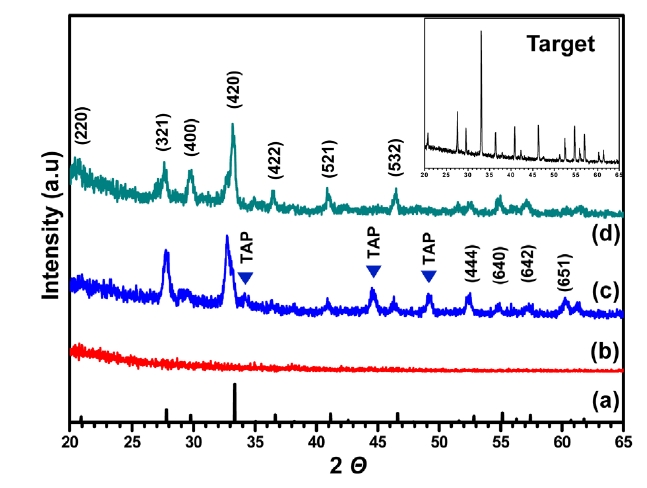
Figure 1 shows XRD patterns of (a) JCPDS data for TAG crystal, (b) as-deposited TAG:Ce thin film and TAG:Ce thin film post-annealed at (c) 700 and (d) 800℃ for 2 hrs, respectively. The as-deposited films were amorphous in nature, and did not represent any crystalline peaks. Post-annealing less than 700℃ did not effectively crystallize the thin film. The thin films started to crystallize when annealed at 700℃ for 2 hrs as shown in (c). However, an intermediate TaAlO3 (terbium aluminum perovskite, TAP) phase coexisted with the TAG phase. Completely crystallized pure TAG phase was obtained after post-annealing at 800℃ for 2 hrs as shown in (d). This post-annealing temperature is somewhat similar to that of citrate-complex derived TAG:Ce powders [5], and significantly lower than that of the conventional solid-state reaction process [15].
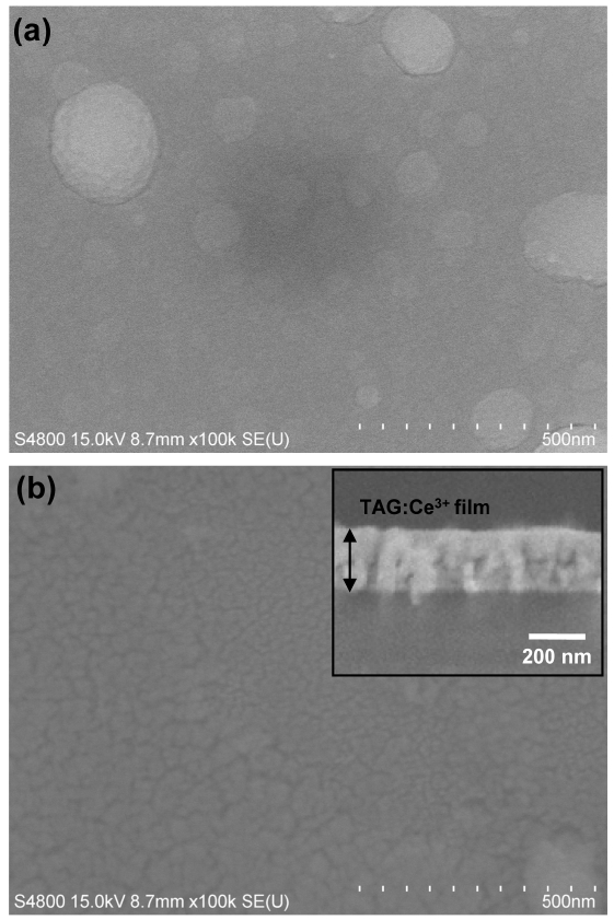
Figure 2 shows the surface morphologies of the TAG:Ce films (a) as-deposited and (b) post-annealed at 800℃ for 2 hrs. The surface microstructure of the TAG:Ce thin films deposited by PLA was affected by a post-annealing process. Indeed, the surface of the as-deposited TAG:Ce thin film exhibits a smooth morphology without particular features. However, after post-annealing treatment at 800℃ for 2 hrs, the surface became rougher resulting from grain growth and formation of particulates as shown in (b). The inset of (b) shows a cross-sectional view of the sample of thickness about 250 nm after annealing at 800℃ for 2 hrs.
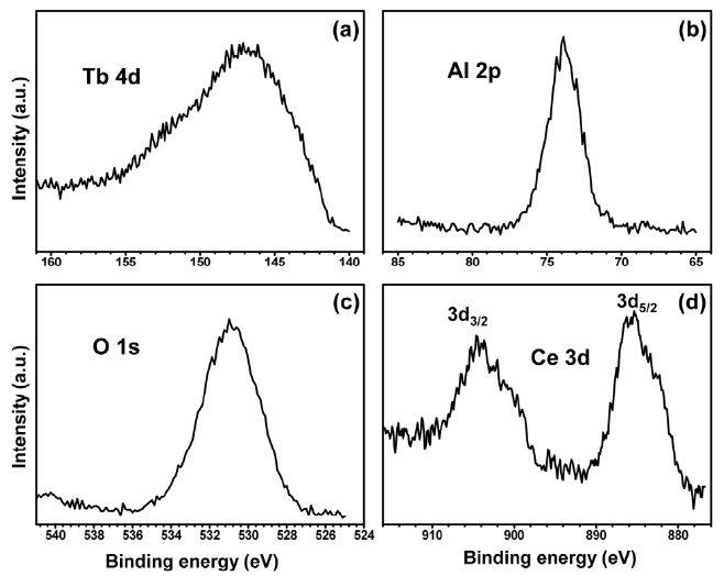
The surface composition of the TAG:Ce thin film post-annealed at 800℃ for 2 hrs was analyzed using XPS. Figure 3(a-d) presents the high resolution XPS spectra of the (a) Tb 4d, (b) Al 2p, (c) O 1s, and (d) Ce 3d. The
binding energies of the Tb, Al, O, and Ce were well in agreement with reported values [16]. The Ce 3d feature in (d) shows a complex structure consisting of Ce 3d5/2 and Ce 3d3/2 spin-orbit doublet around 885 and 904 eV, respecti-
respectively, which is a characteristic property of the Ce3+ ion [17].This spectral feature confirms that the chemical valence of Ce ions doped in the TAG:Ce thin film is trivalent. Moreover, a calculated chemical composition of Ce3+ in the TAG:Ce film post-annealed at 800℃ for 2 hrs was 0.075, which corresponded well to the doping concentration of the bulk target (8 mol%).
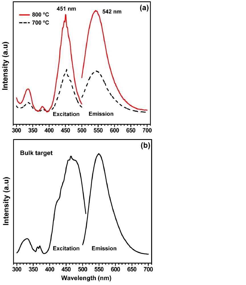
Figure 4(a) depicts the excitation and emission spectra of the TAG:Ce thin film post-annealed after PLA process. The PL spectra of the bulk target used for PLA are presented in (b) for comparison with those of the TAG:Ce thin films. As shown in Fig. 4, both excitation and emission spectral shapes of the TAG:Ce thin films are almost identical to those of the target used for the PLA. The PL intensity of the as-deposited film (not shown) was almost two orders lower than those of the post-annealed thin films. The emission intensity of the TAG:Ce thin film post-annealed at 700℃ for 2 hrs was about 10% of the bulk target. This low PL intensity may originate from incom-plete crystallization and an intermediate TAP phase. However, enhancement of the emission spectrum up to 30% of the bulk target was observed in the sample post- annealed at 800℃ for 2 hrs. This result indicates that low-temperature post-annealing process can remarkably enhance the emission intensity of the TAG:Ce thin film deposited by PLA in room temperature. The PL excitation spectrum of the post-annealed TAG:Ce thin films showed two bands peaking at 335 (weak) and 450 nm (strong) due to the transitions from
In summary, Tb3Al5O12:Ce (TAG:Ce) luminescent thin films were successfully deposited by pulsed laser ablation (PLA) with a low-temperature post-annealing process. XPS analysis showed that the PLA process preserved the chemical bonding property of the target that was effectively transferred to the deposited films after post-annealing at 800℃ for 2 hrs in ambient conditions. Furthermore, the luminescent property was recovered by the low-temperature post-annealing process. The strong emission band around 542 nm was obtained by exciting the