Semiconductor ring cavities offer a large number of applications due to the compact geometry, no need of cleaving and the possibility of integration between active and passive devices [1-10]. Recently, devices with ring cavities have been widely studied and utilized in several different technologies at all levels of cost in fabrication [11-19]. In most semiconductor cavities, the radius should be many times the operating wavelength to attain high quality (Q) factors [14,21,22]. In the case of using these cavities, in other words the multiple resonance case, the closely spaced wavelength resonances are inevitably obtained. However, the narrow free spectral range (FSR) of the output spectra is not desirable in most photonic device applications, such as passive filters and laser cavities. Thus, achieving a moderate FSR or a single mode operation in an optical cavity is essential if it is to be used as an integrated optical component.
One of the possible methods to obtain a large FSR is using the coupled cavities to lase only the common resonance mode between two cavities. Usually, the coupling between cavities or with the waveguide needs a very small gap distance down to sub micrometers due to the high lateral confinement by deep etching. Eventually, we would not be able to avoid an intricate process such as e-beam lithography when use the semiconductor materials. This difficulty limits the fabrication and application of semiconductor ring or disk cavities as the integrated device elements. In our previous work [23], single mode lasing was reported in the multimode interferometer (MMI) coupled square ring cavity, which does not use evanescent coupling. In this work, we focused on the stabilities of the single mode behavior in coupled cavities by varying the ambient temperature and input pump powers.
II. DESIGN, FABRICATION AND MEASUREMENTS
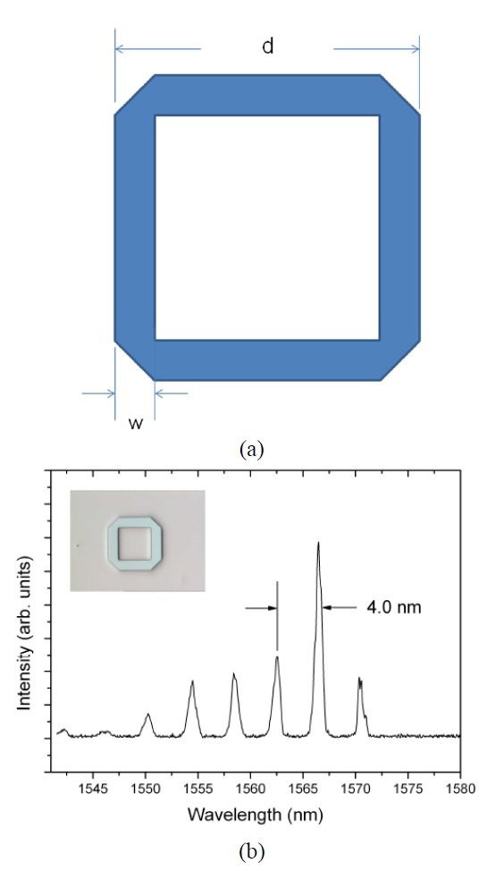
Before the study of the coupled square ring cavity, the single square ring cavity was fabricated and characterized. In figure 1 (a), the schematic diagram of a single square ring cavity is presented and its waveguide width (w) and cavity length (d) are defined. In addition, the output spectrum of the fabricated single cavity and its microphotograph are shown in figure 1 (b). We are going to briefly describe the design, fabrication and measurement processes of the square ring cavity. Details of the entire processes have been described elsewhere [23].
For the proposed semiconductor cavity fabrication, InP/ InGaAsP based semiconductor epitaxial layers were chosen. The active layers consisted of 6 layers of undoped InGaAsP/ InGaAs multiple quantum well (MQW)s with a center wavelength, λ g= 1.55 μm and are sandwiched by n- and p-type InGaAsP confinement layers. p-InP on active layers and n-InP buffer on InP substrate were used as cladding layers.
The devices are fabricated by a standard III-V compound semiconductor process. Particularly, a careful etching process using CH4/H2 reactive ion etching is needed to obtain the refined vertical surface of a device. In addition, the etch depths exceeding 4.2 μm are controlled to laterally confine the travelling wave and to prevent radiation losses into the substrate.
For a measurement of the cavity properties, an acoustooptic Q-switched (10 kHz) Nd:YVO4 laser, wavelength of 1.06 μm, is adapted to optically pump MQWs. With this wavelength, some of the pump light penetrated the clad layer and was strongly absorbed by the MQW layers. The lasing signal from the coupled-cavity was collected through a tapered fiber launched around the cavity corner and inclined to cavity plane in order to measure maximum intensity and its spectrum was analyzed by an optical spectrum analyzer (HP 81818).
The waveguide width (w) of the square cavity, illustrated in the inset in figure 1 (b), is 10 μm and length of the cavity side (d) is 50 μm. The square ring cavity has 45o
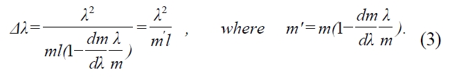
tilted flat corners. When the corners are symmetrically 45o -tilted, closed orbits, formed by total reflections with an incident angle 45o at the corner, are possible. Based on this closed orbit cavity mode, the lasing spectrum of the single square cavity showed multimode and many closely spaced resonance peaks of 4 nm as shown in figure 1 (b). To support this value, the parameter m' was estimated to be 3.55 at 1550 nm by the calculation represented as below. The spacing between the multi-resonant wavelengths can be controlled by varying the cavity length. For the calculations of the resonant wavelengths, the optical path length L can be given as follows;

where

where
This Fabry-Perot-like resonant equation is valid when the cavity sizes are much larger than the operating wavelengths.
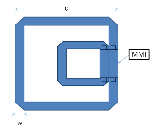
Figure 2 exhibits the schematic diagram of the MMI coupled square ring structure. An MMI is proposed to couple the square ring cavity. Unlike the circular cavity, the straight MMI is the best choice to couple two square
cavities. MMI is known to have self-imaging or power splitting functions by controlling the MMI length [24,25]. As shown in figure 2, a square cavity rests within a larger square cavity. One side of the smaller cavity lies along a side of the larger cavity. Thus, the coupled waveguide width is twice the square waveguide width and can be regarded as an MMI. When the light enters a coupled waveguide region, it suffers abrupt waveguide broadening. Finally, the light intensities are divided and coupled separately into outside and inside cavity.
The main idea is to use the Vernier effect with which it is possible to enhance only one mode by suppressing every other mode existing in a single square ring cavity. The selected modes that fulfill both cavity resonance conditions are significantly enhanced. As a result, the single mode lasing can be expected through the common resonance of two semiconductor cavities.
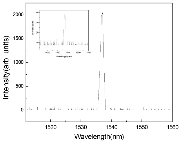
Figure 3 shows the typical lasing spectrum of the fabricated MMI-coupled square cavity by pulsed optical pumping and its logarithmic value of the lased optical intensities in the inset. The device has a specification of an outside cavity length, an inside cavity length and a waveguide width of 50 λm, 20 λm and 4 λm, respectively, and it will be referred to as 50-20-4. From the beam propagation calculation, the coupling ratio into the adjacent cavities was calculated to 0.24 at the center wavelength. Depending on the equations presented above, the FSR of each cavity was calculated as 3.28 nm for the 50 λm-cavity and 8.20 nm for the 20 λm-cavity.
The illustrated lasing spectrum of the MMI coupled cavity in figure 3 represents single mode operation with full width at half maximum (FWHM) of 0.83 nm and a side mode suppression ratio (SMSR) of 24.90 dB, which is the
best result we measured. The center wavelength was measured as 1537.0 nm, which is in the range of the photoluminescence spectrum of the MQW. From these experimental results, single mode operations can be simply obtained in the MMI coupled square cavity.
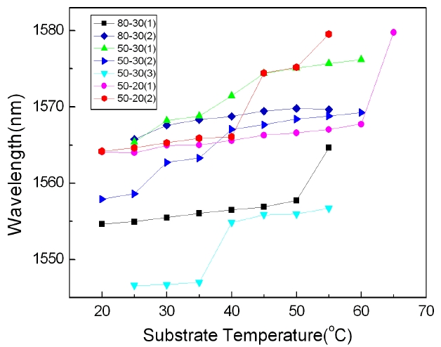
Beside the resonant characteristics, it is important to get the information of the stability of the coupled cavity by changing the temperature and pump optical power. In figure 4, the temperature dependent lasing center wavelengths have been measured for devices with 50-20-6, 50-30-6, and 80-30-6 devices. The temperature of the semiconductor device substrate was controlled by thermoelectric cooler between 20℃ to 65℃. Increasing the temperature, the single mode lasing was maintained within the measured temperature range in spite of the red shift of the center wavelength. Mode hopping was also observed but the hopping temperature and the total amount of hopping distance were not fixed. This can be explained by an effective refractive index change in semiconductors according to temperature change. Except for the mode hopping region, the temperature dependent red shift of the wavelength is too small to be considered as a material dispersion. The value of ~ 1 nm /℃ is comparable to the distributed feedback laser diode [26], which implies that the lasing wavelength is dominantly determined by its structure, not by the material dispersion.
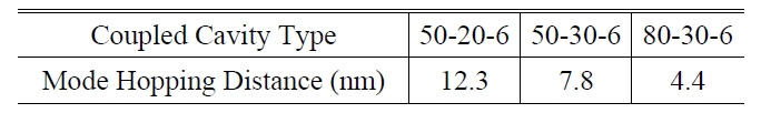
The differences in hopping values categorized by various cavity combinations are summarized in Table 1. In the order of 80-30-6, 50-30-6, and 50-20-6 devices, the hopping
[TABLE 1.] The average mode hopping distance in wavelength for the various devices are summarized

The average mode hopping distance in wavelength for the various devices are summarized
distance has clearly increased. This can be reasonably understood knowing that the mode spacing of the long cavity is smaller than that of the short cavity. As a result, the hopping of the resonant wavelength can get larger as the device size decreases.
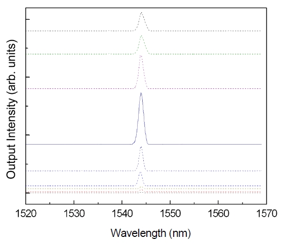
We also investigated the single mode behavior by varying the optical input powers as shown in figure 5. The vertical axis shows linear intensity of the emitted spectra from the cavity. In order to easily compare the lasing characteristics according to pump power, the lasing curves were placed vertically as the pump beam intensity increased.
The input power level was increased several times larger than the threshold average input power level for each measurement step. The threshold pump power of the coupled cavity was measured to be ~2 mW. By increasing the pump power up to ~30 mW, the lasing peak power rapidly increased and the single mode lasing was maintained with an enhanced SMSR of ~20 dB represented as a solid line in figure 5. Beyond this power level, the quality factor (Q)s are gradually degraded in MMI coupled cavities due to a de-tuning effect. It is well known that the Q factors of the microcavities degrade as the pumping power exceeds the optimum power level. From the above result, we found that single mode operations can be maintained on the wide range of pump power.
Design and characteristics of the MMI coupled square cavities were demonstrated using InGaAsP MQW semiconductor layers. The MMI coupled square cavities exhibit single mode lasing spectra as expected. It was also found that the single resonance mode was preserved for a large ambient temperature range in spite of mode hopping. For the pump power change, the lasing spectrum was analyzed and the single mode lasing was maintained for the wide range of input optical power. From the experimental results, it was concluded that single mode lasing in MMI coupled square cavities can be obtained by relatively simple fabrication processes and the cavities can also be applied to any integrated passive or active building blocks in semiconductor devices.