We present a method that enables dual threshold voltages in a vertical alignment liquid crystal device, through which the gamma shift can be reduced with no subsequent decrease in the contrast ratio. By forming polymer layers, the threshold voltage shift is accomplished through the utilization of the voltage drop effect. We expect that the proposed method can be applied to the conventional 4-domain mode in order to achieve an 8-domain mode without the need for complex driving schemes.
Liquid crystal displays (LCDs) have been widely used in various areas due to their excellent features, i.e. their lightness, high resolution, low power consumption, etc. There are several popular modes for LCDs, such as the twisted nematic mode, the vertical alignment (VA) mode, and the in-plane switching mode [1-3]. Amongst these modes, the VA mode displays a superior dark state, through which a high contrast ratio can be realized due to the fact that the liquid crystals (LC) molecules are aligned perpendicularly to the substrates in their initial state. However, LCs in a single domain VA mode tilt down in only one direction in the presence of an applied voltage, resulting in asymmetric viewing angle characteristics. The multi-domain vertical alignment (MVA) mode has been proposed in order to overcome this problem, however, the MVA mode still suffers from off-axis gamma shifts [4].
In order to decrease the gamma shift, various approaches have been presented [5-6]. However, additional thin film transistors and data lines are required, resulting in a complex manufacturing process which leads to high costs. In order to simplify the manufacturing process, an 8-domain PVA mode driven by a single transistor has been proposed, which achieves fabrication by introducing two different pretilt angles within a pixel [7]. Although the manufacturing process is easier, the contrast ratio may suffer because of the inherently high pretilt angles. A multi-domain VA device using dual threshold voltages has been proposed as well [8]. However, only numerical results were given; it is difficult to apply the required deposition method with a sputtering machine when fabricating large-sized LCD panels.
In this paper we present a method by which we can reduce the gamma shift in a VA cell with no decrease in the contrast ratio. By forming a polymer layer on each substrate the realization of different threshold voltages in a VA cell becomes possible. We expect that the proposed method can be applied to the conventional 4-domain mode in order to achieve an 8-domain mode without the need for complex driving schemes.
II. CONFIGURATIONS AND PRINCIPLE OF OPERATION
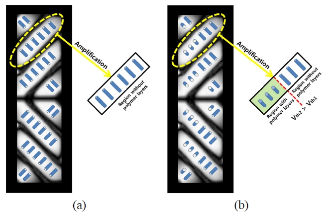
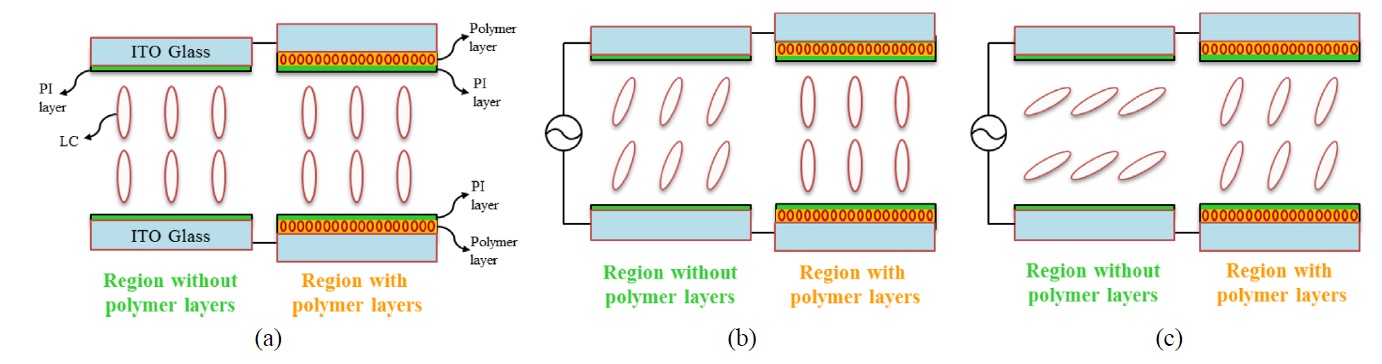
Figure 1 shows the operational principles of the proposed VA mode. A polymer layer was formed on each substrate in some region of each pixel before adding the polyimide layer, whereas no polymer layer is formed in the other region of the pixel. In the initial state LCs are aligned
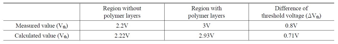
Measured and calculated threshold voltages of the region without polymer layers and the region with polymer layers
vertically in both regions, as shown in Fig. 1(a). The LCs in the region without polymer layers tilt down, as shown in Fig. 1(b), when a voltage is applied with a magnitude between the threshold voltage of the region without polymer layers and that of the region with the polymer layers; the LCs in the region with the polymer layers remain in the initial state. When the applied voltage exceeds the threshold voltage of the region with the polymer layers, its LCs also tilt down, as shown in Fig. 1(c). In this manner we create two different threshold voltages within each pixel, resulting in a multi-domain structure. As the applied voltage increases further, a difference in the transmittance can be observed until the transmittance of the cell with the polymer layers reaches its maximum.
The applied voltage V is divided into two layers: the VLC across the LC layer and the Vin-cell across all of the other layers [9]. This relationship is described by:
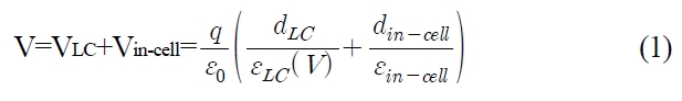
where q is the charge density, dLC is the cell gap of the LC, din-cell is the thickness of the in-cell layer, εLC is the dielectric constant of the LC molecules, and εin-cell is the dielectric constant of the in-cell layer. In the area without polymer layers, the operating voltage is related to the voltage applied to the LC layer (VLC) and the voltage applied to the polyimide layer (VPI). In the area including polymer layers, the operating voltage is related to the voltage applied to the LC layer (VLC), the voltage applied to the polyimide layer (VPI), and the voltage applied to the polymer layer (Vpolymer). We can use the following equation
to compare the operating voltages of the region without polymer layers and the region with polymer layers.
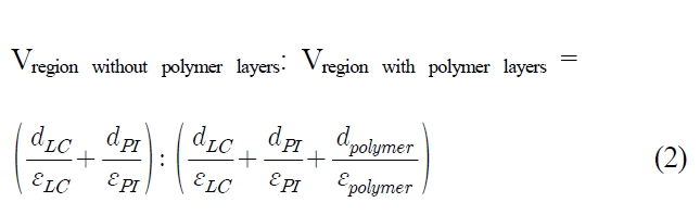
Due to the differences in the dielectric constants, we gain different threshold voltages through the use of the proposed method. We can apply this method to a conventional 4-domain mode (see Fig. 2(a)) to obtain the 8-domain mode by using two different threshold voltages shown in Fig. 2(b).
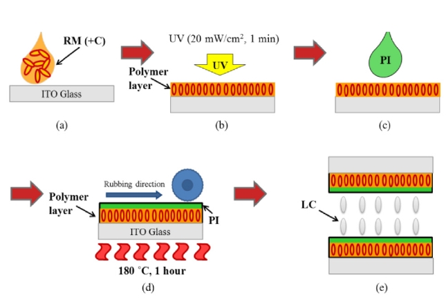
Figure 3 shows the fabrication process for the proposed VA cell. In order to verify the attributes of the polymer layer in the proposed method, we fabricated a VA cell with a polyimide layer coated polymer layer. We also fabricated a VA cell without a polymer layer for comparison. First, the monomer was coated, as shown in Fig. 3(a). In this device, we used a reactive monomer composite (RMS03-015, εr =3.5, Merck). The reactive monomers were spin-coated onto ITO glass substrates. The spin coating was done for 30 seconds at 3000 rpm. The monomers were then polymerized under ultraviolet light irradiation in order to form the polymer layer, and cured at 20 mW/㎠ for 1 min, through which the polymer layer was formed, as shown in Fig. 3(b). The thickness of the formed polymer layer was 0.5 μ m. After the curing process, the polyimide used for the vertical alignment was coated onto the substrates, as shown in Fig. 3(c). The coating process was divided into two steps: 1100 rpm for 15 seconds and 4500 rpm for 45 seconds. In order to eliminate the solvents in the polyimide, the substrates were pre-baked at 120° C for 3 minutes and then post-baked at 180° C for 1 hour, as shown in Fig. 3(d). The rubbing process was performed in order to align the LCs in an identical direction in the presence of an applied voltage. The cells were assembled with the cell gap fixed at 5 μm by using silica spacers and sealed together using epoxy. Finally, negative LCs (△n = 0. 077, △ε = - 4, Merck) were injected into the empty cell, as shown in Fig. 3(e). A reference cell without polymer layers was fabricated using the same fabrication process except for the polymer layers process step.
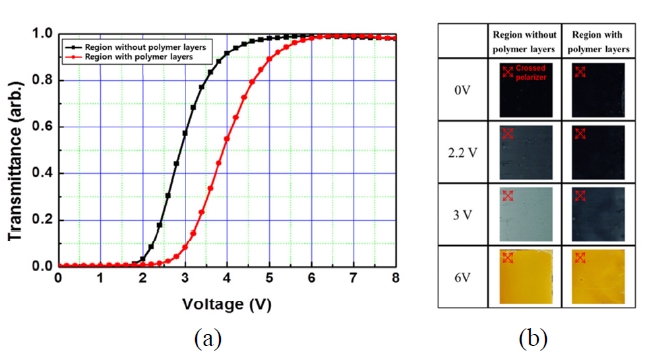
In order to confirm the electro-optic characteristics of the fabricated cells, we measured the voltage-transmittance (V-T) curves of each VA cell, as shown in Fig. 4(a). We used a white light source (Model C4251, Photal Otsuka Electronics) to measure the V-T curve. The threshold voltage was defined to be the applied voltage giving 10% of the maximum transmittance. The voltage applied to the LCs was ranged from 0 to 8 V. Both cells show good dark characteristics in the initial dark state because the LCs were perfectly vertically aligned in both cells. As the applied voltage increased, the two cells showed a threshold voltage difference of 0.8 V. The threshold voltage of the cell with the polymer layers was higher than that found for the reference cell due to the voltage drop effect. The difference in the transmittance of each cell was maintained until the transmittance reached its maximum, which was obtained at an applied voltage of 6 V. Although the driving voltage was different, the maximum transmittance for both cells was very similar.
Figure 4(b) shows images of the fabricated VA cells
under crossed polarizers at various applied voltages. The images of the cell without polymer layers are shown on the left, whereas those of the cell with the polymer layers are shown on the right. Since the cell with the polymer layers has a higher threshold voltage than the cell without polymer layers, the bright state of the cell with polymer layers is observed to be at a higher applied voltage, as shown in Fig. 4(b). However, both cells show similar bright states at an applied voltage of 6 V. We compared the measured threshold voltages with the threshold voltages calculated using equation (1) when there are polymer layers on both of top and bottom substrates. The measured values were similar to the calculated values, shown in Table 1. Although each VA cell was fabricated separately in this experiment, we can expect a gamma shift improvement from the two different threshold voltages when we form polymer layers on a section of each pixel.
We present a method that can reduce the gamma shift through the use of the voltage drop effect. By forming a polymer layer on a section of each pixel, different threshold voltages can be obtained in a VA cell. We expect that the proposed method can be applied to the conventional 4- domain mode in order to achieve an 8-domain mode without the need for complex driving schemes.