Electrically tunable focusing liquid crystal (LC) lenses are reviewed in this paper. The distribution of the orientations of LC directors which is controlled by electric fields results in a distribution of refractive indices of LC directors. The incident light can be modulated by the electrically tunable lens-like phase difference of the LC lens. We introduce the basic operating principles of LC lenses and discuss the structures of LC lenses. The major challenges of LC lenses are also discussed. We believe this paper provides a guideline for basic understanding of LC lenses.
Liquid crystal (LC) lenses which are active optical elements with electrically tunable focal lengths have many applications, such as three-dimensional displays, imaging systems, microscopes,zoom systems and optical tweezers [1-9]. The features of the low power consumption and the thin thickness of LC lenses are promising for portable devices. The main mechanism is that an incident plane wave propagates in a LC lens experiences a lens-like phase difference due to the distribution of orientations of LC directors. The wave front of the incident plane wave is then bent as a converging or a diverging spherical wave. LC lenses basically could be categorized according to the aperture size. LC lenses with the small aperture size (<1 mm) are suitable for applications of microlens arrays and LC lenses with large aperture size (>1 mm) are suitable for portable devices, such as cell phones and pico projectors [9,10]. In this paper, we review the technology of the LC lenses with large aperture size. We start from the operating principles and review all the structures of the LC lenses. We believe this paper provides a guideline for the researchers and engineers for basic understanding of LC lenses.
2. THE OPERATING PRINCIPLES OF LC LENSES
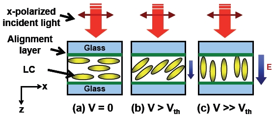
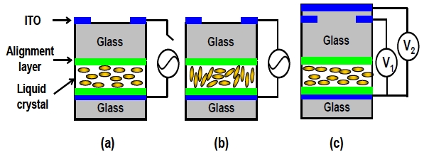
Rod-like structured LCs are fluidic-anisotropic materials. Generally speaking, LCs are confined in a LC cell which comprises two indium tin oxide (ITO) glass substrate coated with alignment layers, as shown in Fig. 1(a). Figures 1(a-c) show the electrically tunable refractive indices of the LC cell. As the electric field (E) applies to the LC cell, the electric field results in a torque to the induced dipole moment of the LC molecules and change the orientations of LCs, as depicted in Fig. 1(b). The LC molecules are parallel to the electric field at a high electric field, as depicted in Fig. 1(c). When the polarization of incident light is x-linearly polarized, the effective refractive index (neff) can be expressed as [11]:
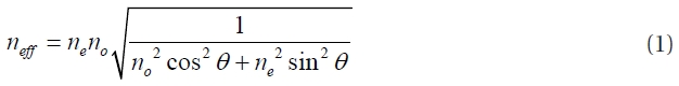
where Θ is the tilt angle between the LC directors and the polarization of the incident light, ne and no are the extraordinary and the ordinary refractive indices of LCs, respectively. From Eq. (1), the effective refractive index could be changed from ne to no as the tilt angle increases by applying electric fields.
To mimic a solid lens by using LCs, a lens-like phase difference of LCs can be arranged by means of the distribution of orientations of LC directors or the distribution of the refractive indices
of LC. The wave front of an incident plane wave propagating in a LC lens is converted to a convergent or a divergent spherical wavefront. As a result, the LC lens acts as the positive lens or negative lens. When the distribution of orientations of LC directors is adjusted by the applied electric fields, the curvature of the spherical wave fronts is electrically controllable and so is focal length of the LC lens which can not be achieved by the conventional solid lenses. Here, we simply classify the LC lenses into two groups, one is the LC lens with an inhomogeneous cell gap and the other is the LC lens with a homogeneous cell gap.
2.1 A LC lens with an inhomogeneous cell gap
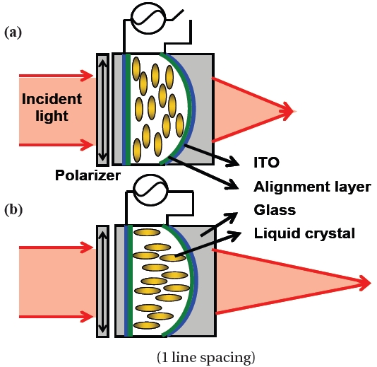
Figures 2(a) and (b) show the operating principles and the structure of the LC lens with an inhomogeneous cell gap [12]. The LC lens consists of a polarizer, a LC layer, the conventional concave glass lens and the planar glass substrate. Both of the glass lens and glass substrate are coated with transparent electrodes and alignment layers. The alignment layers are mechanically buffered in anti-parallel directions. The polarizer is used to filter out the ordinary wave of incident light. On a basis of geometric optics, the focal length of the LC layer with the curve surface (fLC) can be expressed as [11]:
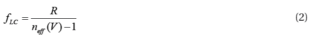
where R is the radius of curvature of the concave glass lens, neff is a voltage-dependent effective refractive index of the LC layer. The total focal length of the LC lens is composed of two sublenses:one is the LC layer and the other is the concave glass lens. The total focal length of the LC lens (f(V)) can be written as [12-19]:
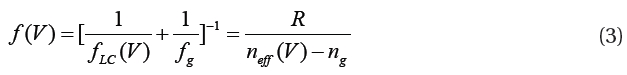
fg is the focal length of the concave glass lens,
2.2 A LC lens with a homogeneous cell gap
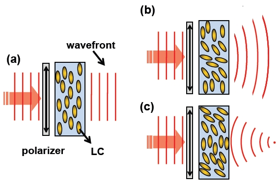
Figure 3 shows the operating principles of the LC lens with a homogeneous cell gap. In Fig. 3(a), the incident light propagates through the polarizer whose transmissive axis is parallel to the rubbing direction of the LC cell. LC directors are aligned homo-geneously. The wavefront of the incident light does not change by the LC lens, as shown in Fig. 3. As a result, the focal length of the LC lens is at infinity. In Figs. 3(b) and (c), the incident wavefront after the polarizer is bent because of the distribution of orientation of LC directors and then turns out a divergent or a convergent spherical wavefront. The LC cell acts as a negative lens in Fig. 3(b) or a positive lens in Fig. 3(c). The distribution of orientation of LC directors can be controlled by applying inhomogeneous electric fields.
When the phase distribution induced by the LC lens is parabolic which means the LC lens acts as a conventional thin solid lens, the focal length of the LC lens can be expressed as [20]:
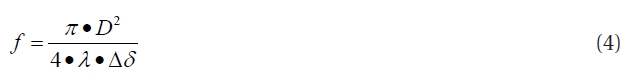
where D is the aperture width of the LC lens, λ is the wavelength, the phase different (Δδ) between the border and center part of the aperture can be expressed as:
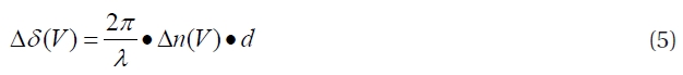
where d is the cell gap of the LC lens, Δn(V) is the difference of the refractive index between the center part and the border part of the aperture. From Eqs. (4) and (5), the focal length of the LC lens depends on voltage due to the electrically tunable orientations of LC (or the refractive indices). Δδ can be positive or negative. The maximum of Δn equals to
3.1 LC lenses with an inhomogeneous cell gap
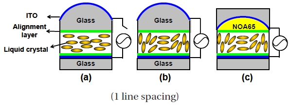
The first LC lens was invented by Sato in 1979 [12]. Sato demonstrated a LC lens with an inhomogeneous cell gap in Fig. 2. The focal length of the LC lens is short; however, the thick and nonuniform cell gap causes slow response time. For improving the response time of the LC lens, switching polarization states of the incident light can change the focal length of LC lenses for extraordinary wave (e-wave) and ordinary wave (o-wave) [12,31,32]. To switch the polarization states of the incident light, a twisted nematic (TN) cell can be placed in front of the LC lens, for example. Therefore, the actual response time of the LC lens depends on the response properties of the TN cell. Besides, different LC materials which have fast response time can also help improving response time in this design of the LC lens [16,19]. In this structure of the LC lens, the major disadvantage is that the inhomogeneous cell gap results in the alignments difficulties of LC directors. Figure 4 illustrates the LC directors near the curved surface. Without applying a voltage, as shown in Fig. 4(a), the LC directors do not tilt in the same direction. After applying a voltage, the LC directors reorient in the different directions and then result in a disclination line, as shown in Fig. 4(b). The disclination lines and the scattering degrade the image quality. Therefore, the LC lens with an inhomogeneous cell gap is usually for the applications of microlens arrays [13,14,16-19] or of the Fresnel lenses [31,32].
3.2 LC lenses with a hole-patterned electrode
Compared to the LC lens with an inhomogeneous cell gap, the
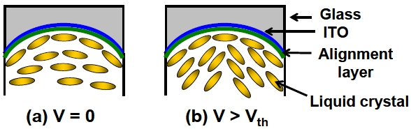
LC lens with a homogeneous cell gap can be more compact and lower scattering for better LC alignment. However, the design of electrodes of the LC lens with a homogeneous cell gap is more complicated. For generating the lens-like phase difference, the electric fields should be non-uniform in order to obtain a distribution of refractive indices of the LC layer. The hole-patterned electrode is a way for providing non-uniform electric fields [21]. The LC layer is sandwiched between the plane-paralleled electrodes. One of the electrodes is etched with a hole-pattern. As a result, when voltages apply to those two electrodes, the inhomogeneous electric fields result in a lens-like distribution of phase difference in LC layer and then the incident light can be focused by the LC layer. When the aperture size of the LC lens is larger than 1 mm, the electric field does not distribute in the central area of the hole area and then the focusing effect of the LC lens is poor. For realizing a LC lens with a large aperture size, a glass substrate as a dielectric layer is added between the holepatterned electrode and the LC layer [21-30,33-36], as illustrated in Figs. 5(a-c). The purpose of the inserted dielectric layer is to extend the distribution of the electric fields to the whole aperture region. In Fig. 5(a), no focusing effect of the LC lens at V = 0. In Fig. 5(b), the voltage distribution results in the oriented distribution of LC directors at V > Vth. The LC lens has a focusing effect. The LC lens has a positive and shortest focal length when the LC directors near the boundary of the hole are perpendicular to the glass substrate and the LC directors in the central area of the hole are parallel to the glass substrate, as shown in Fig. 5(b). As the voltage increases, the LC directors in the central area continue rotating and the focal length of the LC lens turns out longer. The focal length is infinite while all of the LC directors are perpendicular to the glass substrate as V ≫ Vth.
To obtain a LC lens which could be switched between a positive lens and a negative lens, two-voltage structure should be adopted, as depicted in Fig. 5(c). In Fig. 5(c), the LC lens is a positive lens when V1>V2, and the LC lens is a negative lens when V2 > V1 [24-27]. The hole-patterned electrodes can also be divided into many electrodes, or sub-electrodes, for adjusting the phase profile precisely [26,27]. For most applications, the LC lens with fast response time and short focal length is required. Multiple LC layers, special driving methods [33-35] and different LC materials [37] are demonstrated for improving the response time. By using a built-in planar polymeric lens to shift the focal length, the LC lens with a built-in planar polymeric lens can obtain short focal length [38].
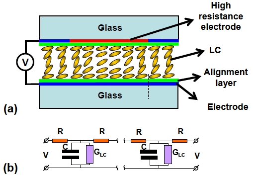
The dielectric layer causes the high operating voltage of the LC lens. Improving the dielectric layer with small thickness and weak conductive properties can reduce the operating voltages [28-30,33]. Another method to lower the operating voltage is called modal LC lens, as depicted in Fig. 6(a) [39-47]. The modal LC lens is based on the structure of the LC lens with a holepatterned electrode, but the hole-patterned electrode is coated with a high resistive film. The high resistive film can be treated as many resister R in series. The LC layer can be treated as capaci-
tance CLC and the small conductance GLC in parallel. The equivalent circuit is shown in Fig. 6(b). When we applied an alternating current (AC) voltage (V) to the LC lens, the current through the capacitance CLC induces the voltage drop on the resister R. Therefore, the voltage across the LC layer decreases from border part to center part of the aperture and the modal LC lens focuses the incident light. The focal length of the modal LC lens is the frequency dependent. The high frequency and uniform resistive film increases the difficulties of the driving method and fabrication process.
3.3 LC lenses with a curved electro
Instead of a hole-pattern electrode, the LC lens with a curved electrode is a method to realize the tunable focusing properties meanwhile the LC lens has uniform cell gap and inhomogeneous electric fields [48-52]. The structure of the LC lens with a curved electrode is illustrated in Figs. 7(a-c). The planar-convex glass lens coated with the ITO is the curved electrode, as shown in Fig. 7(a). Similar to the LC lens with an inhomogeneous cell gap, the focal length is contributed from two sub-lenses: one is the planar-convex glass lens and the other is the LC layer. The initial focal length is determined by the focal length of the planar-convex glass lens at V = 0. The equivalent circuit of the LC lens can be treated as two capacitances in series: one is the planar-convex glass substrate and the other is the LC layer. When we applied the voltage (V) to the LC lens, we can derive the voltage across the LC layer VLC as [49]
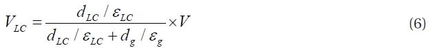
where εLC and εg are the dielectric constants of the LC layer and the glass substrate. dLC and dg are the thicknesses of the LC layer and the glass lens. Since the thickness of the planar-convex glass lens is thicker at center region, the voltage of the LC layer at the border region is higher than the center region. Therefore, the curved electrode generates the inhomogeneous and circularly symmetric electric fields. The LC lens has a positive focal length, as Fig. 7(b) shows. The advantage of this design is no disclination lines. However, the glass lens with a curved electrode results in the thick thickness and the focal length at V = 0 (or initial focal length). To remove the initial focal length, a UV curable polymer whose refractive index is as same as glass lens is used to flatten the curved surface, as shown in Fig. 7(c) [50,51]. By properly designing the shape of the curved electrode, the LC lens with a curved electrode can have better image quality and shorter focal length than hole patterned electrode [51,52].
3.4 LC lenses with planar electrodes
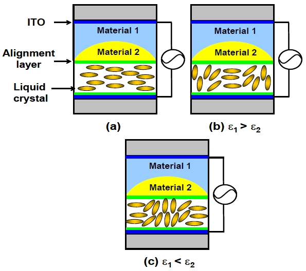
Figure 8 shows the structure of the LC lens with planar electrodes.In order to generate inhomogeneous electric fields, the dielectric layer is inserted between LC layer and a planar electrode. The dielectric layer consists of two materials: Material 1 and Material 2 with the dielectric constant ε1 and ε2, respectively. The spatial-dependent thicknesses of Material 1 and Material 2 are d1 and d2. The refractive indices of Material 1 and Material 2 are the same. Thus the focal length of the LC lens is determined by the focal length of the LC layer only. The focal length is infinity without the applied voltage, as Fig. 8(a) shows. The structure of the LC lens can be treated as three capacitances in series: Material 1, Material 2 and the LC layer. When the voltage (V) is applied to the LC lens, the voltage across the LC layer at the center part is Vc and the border part is Vb . Vb and Vc can be expressed as[53,54]:
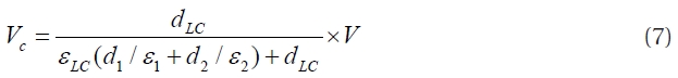
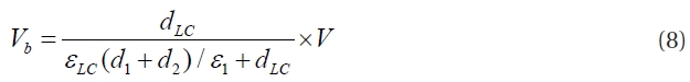
The voltage difference between the center part and the border part comes from the dielectric layer. The LC lens can be the positive lens or negative lens when ε1 > ε2 or ε1 < ε2 as shown in Figs. 8(b) and (c). From Eqs. (7) and (8), reducing the thickness of the dielectric layer or increasing the difference between two dielectric constants can reduce the operating voltage.
Except the dielectric layer, two methods can also realize the LC lens with planar electrode. One is using the photoalignment method to control the distribution of pretilt angles in the LC cell [55-59]. The other method is to use the polymer stabilized LCs [60-63]. By controlling densities of the polymer networks which provides anchoring energy to the LC directors, the tilt angles of the LC are spatially different under an applied voltage. By using the circularly symmetric distribution of polymer networks, the LC lens can also focus the light with planar electrodes.
3.5 LC lenses with pixelated electrodes
The aberration and the image quality of the LC lenses are determined by the distribution of the electric fields. For precisely controlling the distribution of the electric fields, the pixelated electrode design is a way to control the electric fields pixel by pixel [64-70]. The larger numbers of the electrodes have, the better image quality of the LC lenses can have. However, the pixelated electrodes cause the complicated driving scheme and difficulties of fabrication. Adding the resister between the adja-
[Table 1.] Summary of the LC lenses.
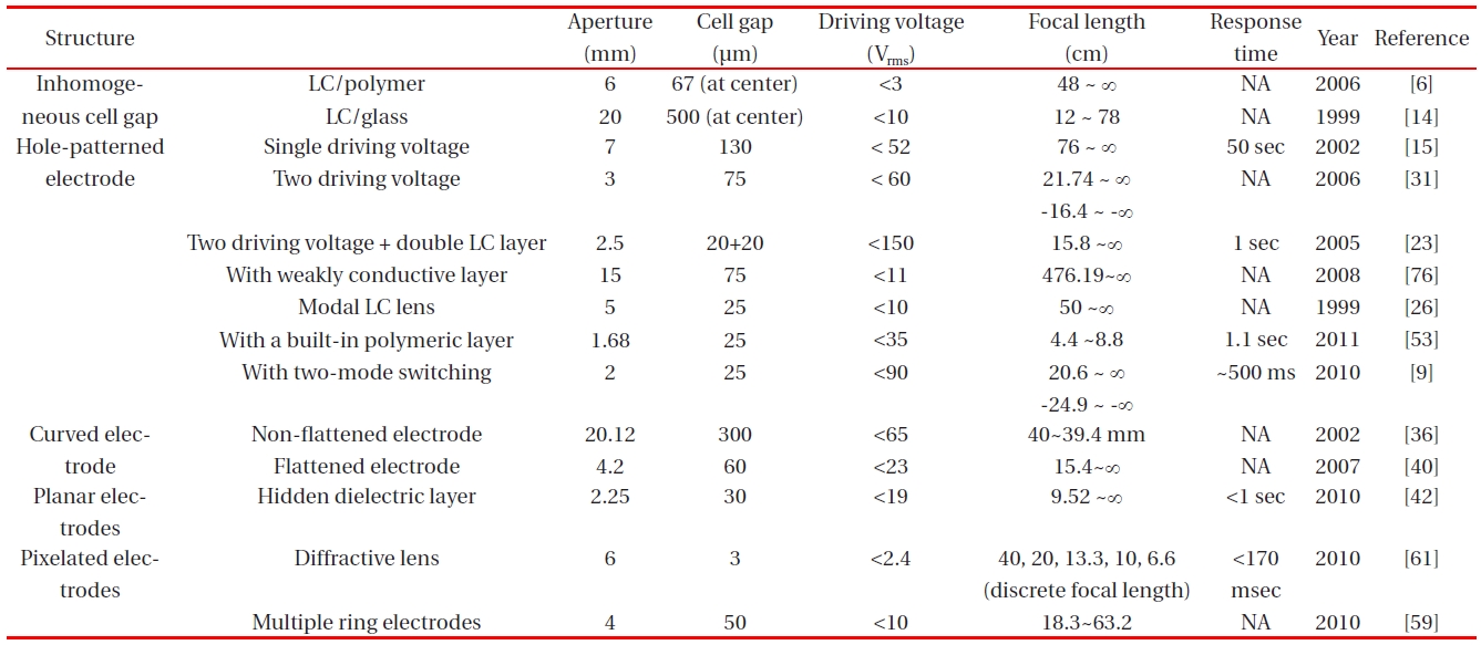
Summary of the LC lenses.
cent electrodes can simplify the driving scheme and provide the smooth distribution of electric field [65-67]. The image quality and diffraction efficiency can be improved by dividing electrodes into two groups: odd and even electrodes, and then two groups are separated by the silicon oxide [65-70]. The gap between adjacent electrodes can be ignored and thus increase the diffractive efficiency and tolerance of the line width. Generally speaking, the fabrication process is the main challenge of the LC lens with pixelated electrodes.
The main challenges of LC lenses are to obtain the large apertures, fast response time, and large electrically tunable focal range. Since the focal length is proportion to the square of the aperture size, the LC lens with a large aperture requires a large phase difference in order to keep the same focal length as the
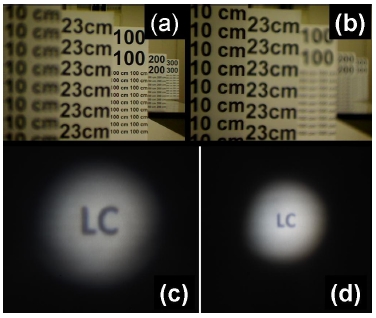
LC lens of a small aperture. However, the large phase difference requires a large cell gap. Increasing the cell gap can enlarge the phase difference, but the response time is slow. By using two-modes switching of the LC lens with a hole-patterned electrode, the LC lens can have large tunable focal range (~300 cm to 10 cm) while maintaining fast response time (~500 ms) [9]. Figures 9(a) and (b) shows the image performance of two-modes switching for the objective distance of 300 cm and 10 cm [9]. However, for the aperture size is larger than 1 cm, the new structure of LC lenses are still need to be developed.
Polarization dependency of the LC lens needs to be solved for applications because optical efficiency decreases by a polarizer. Several polarization independent LC phase modulations are demonstrated or proposed for achieving polarizer-free LC lenses, such as the residual phase modulations [71-74], optical isotropic materials (blue phase LC) [37], or double-layered structure [33-35,75,76].
Table 1 summarizes the published LC lenses. The thickness of the dielectric layer in the LC lens with a hole-patterned electrode is thinner and the operating voltage of the LC lens is smaller. We can choose the Fresnel zone lens to have fast response time and large aperture size, but the focal length can not change continuously. The LC lens with a curved electrode can achieve large aperture but the response time is slow. We can use other LC materials to improve the response time, such as ferroelectric LCs, dual frequency LCs and blue phase LCs. The other method to improve the response time is to divide the cell gap by using a thin glass substrate, but the thin glass substrate causes the structure fragile and complicated.
We have reviewed the LC lenses, including the operating principles and the structures. Actually many photonic applications based on the LC lenses are also developing. For example, the electrically tunable focusing pico projection system using one LC lens is demonstrated [10]. The electrically tunable optical zoom system can be also achieved by using two more LC lenses [5]. We expect the blooming applications of the LC lenses.


![The image performances of the electrically tunable focusing image system by using a liquid crystal (LC) lens. The objective distance is at (a) 300 cm and (b) 10 cm [9]. The image performances of the electrically tunable projection system with optical zoom by using LC lenses for (c) zoom-in and (d) zoom-out the image.](http://oak.go.kr/repository/journal/11440/E1TEAO_2011_v12n6_234_f009.jpg)