A simulation study of a current-mode direct current (DC)-DC boost converter is presented in this paper. This converter, with a fully- integrated power module, is implemented by using bipolar complementary metal-oxide semiconductor (BiCMOS) technology. The current-sensing circuit has an op-amp to achieve high accuracy. With the sense metal-oxide semiconductor field-effect transistor (MOSFET) in the current sensor, the sensed inductor current with the internal ramp signal can be used for feedback control. In addition, BiCMOS technology is applied to the converter, for accurate current sensing and low power consumption. The DC-DC converter is designed with a standard 0.35 μm BiCMOS process. The off-chip inductor-capacitor (LC) filter is operated with an inductance of 1 mH and a capacitance of 12.5 nF. Simulation results show the high performance of the current-sensing circuit and the validity of the BiCMOS converter. The output voltage is found to be 4.1 V with a ripple ratio of 1.5% at the duty ratio of 0.3. The sensing current is measured to be within 1 mA and follows to fit the order of the aspect ratio, between sensing and power FET.
The integrated current DC-DC converter is appropriate for use in many applications, such as portable, display, and cellular applications. The display driver circuit requires an integrated converter to power up digital logic circuits and to convert un-regulated DC input into controlled DC output at a desired volt-age level. The increasing demand of the converter is especially apparent with regard to battery-operated mobile phones. In a cellular phone, for instance, a switch-mode regulator is used to boost voltage. Low voltage operation is an intrinsic circuit characteristic for increased battery efficiency.
Compared to CMOS technology in an integrated converter circuit, bipolar complementary metal-oxide semiconductor (BiCMOS) [1,2] technology can provide the advantage of high current-driving capability and amplifier gain. As its name im-plies,it combines bipolar and CMOS circuits in one integrated circuit (IC) chip.
It combines the low power and high input impedance of CMOS with the high current-driving capability of a bipolar transistor. Specifically, CMOS--although a nearly ideal circuit in many respects--has limited current-driving capability. However, bipolar junction transistor (BJT) is capable of large output currents by virtue of much larger trans-conductance. The controller block in an integrated DC-DC converter usually includes an error amplifier, comparator, current sensor, etc. The error amplifier and current sensor require low on-resistance and high gain in order to obtain a signal of fast transient response and high sensing accuracy. BiCMOS technology is well-suited to the implementation of high-performance circuits.
A current-mode boost converter [3,4] is usually composed of a
feedback network, a switching element, and an output filter. The feedback network is an on-chip integrated circuit for current-mode pulse width modulation (PWM) control. By using the properties of bipolar transistor, a high performance control circuit can be manufactured. The BiCMOS control circuit enables accurate sensing of the inductor current with high frequency and current-driving capability.
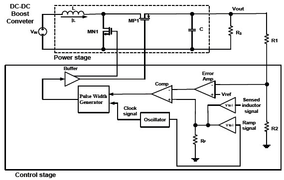
Figure 1 shows the structure of a current-mode boost converter with an off-chip inductor-capacitor (LC) filter. The converter is composed of a power stage and feedback network. In order to provide low power and a fully -integrated power module, a monolithic current-mode DC-DC boost converter, with on-chip current sensor for feedback control, has been designed, with standard 0.35 μm BiCMOS process. All power switches, feedback circuits, and current-sensing circuits are designed on-chip. The off-chip inductor and capacitor are required for the low pass filter. Off-chip LC filters are designed with an inductance of 1 mH and capacitance of 12.5 nF. The output voltage is scaled down by R1 and R2. The scaled voltage is compared with the reference voltage before being fed into the error amplifier. The output of the error amplifier, compensation ramp, and sensed inductor current signal will pass through the comparator and S-R latch in order to define the duty ratio. The duty ratio controls the switching times of the power transistors such that a negative feedback is achieved to regulate output voltage. Although current-mode control is superior to voltage-mode control, there are many difficulties with the circuit realization of the current-sensing function [5,6]. Many approaches to current sensing technology have been proposed, but poor current-sensing accuracy, efficiency degradation, and complicated circuit implementation are problems with IC design. Therefore, the method of sense MOSFET in current- sensing is proposed for a low-voltage current-mode boost converter. The circuit is operated with op-amp in the BiCMOS circuit.
In this work, a current-mode DC-DC boost converter is presented, with standard 0.35 μm BiCMOS process. The proposed circuit is tested by post-layout simulation and is expected to show superior performance compared with the CMOS circuit. The functional and layout simulation are mostly completed by Cadence NC-veirlog and Hspice. The physical design is verified by Calibre and Virtuso.
Current sensing is one of the most important functions of the current-mode DC-DC converter. The DC-DC converter senses the inductor current for over-current (over-load) protection, regardless of the type of feedback control. Additionally, the sensed current is utilized for loop control in the converter. As instantaneous changes in the input voltage are immediately reflected
in the inductor current, mode control can be used to determine when to switch between continuous-conduction mode and discontinuous-conduction mode. This results in an overall increase in the efficiency of the DC-DC converter. The method of sense MOSFET (SENSEFET) is the practical technique for current-sensing in the power MOSFET application [7-9]. The technique is to build a current sensing FET in parallel with the power MOSFET. The effective width of the SENSEFET is significantly less than the power FET. The width of the power MOSFET should be at least 100 times the width of the SENSEFET to guarantee that the power consumption in the SENSEFET is low and quasi-lossless. The voltages at the sources of SENSEFET and power FET should be equal in order to eliminate current mirror non-ideality resulting from channel length modulation. The op-amp is used to force the voltages of VA and VB to be equal. As the width ratio of the main MOS-FET and SENSEFET increases, the matching accuracy of the FETs declines. As the current ratio in SENSEFET circuits is in order of hundreds, even a low-degree coupling between power MOSFET and SENSEFET circuits can induce significant error, and large spikes are expected in the sense signal during the switching period. Therefore, proper layout schemes should be considered in order to minimize the reactive components in power MOSFET and SENSEFET circuits.
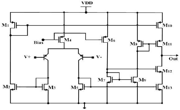
BiCMOS technology combines bipolar and CMOS circuits in one IC chip. The aim is to combine the low power, high input impedance, and wide noise margins of CMOS with the high current-driving capability of bipolar transistors. CMOS, although a nearly ideal logic-circuit technology in many respects, has limited current-driving capability. This is not a serious problem when the CMOS gate has to drive a few other CMOS gates. However, BJT is capable of a large output current by virtue of its large transconductance. A practical illustration of this can be identified in the emitter-follower output stage of emitter-coupled logic (ECL). The high current-driving capability contributes to making ECL much faster than CMOS, at the expense of high power consumption. As BiCMOS technology is well-suited to the implementation of high-performance analog circuits, it makes possible the realization of both analog and digital functions on the same IC chip. The error amplifier and current-sensing circuit illustrated in Figs. 2 and 3 are designed with BiCMOS technology in order to achieve the low power and high input impedance with high current-driving capability of BJT. The error amplifier in Fig. 2 is the cascoded operational transconductance amplifier (OTA) and usually includes a compensation circuit to obtain the stability of frequency response and fast response-time. The com-pensator is used to generate poles and zeros to yield a sufficient phase margin for high stability. The current-mirror type OTA has a p-MOS differential-amplifier, cascade bias, and source-follower. The differential-amplifier and source-follower are used to obtain high transconductance and output resistance, which
are important parameters for stable phase margin in frequency compensation.
The control-to-output transfer function contains two poles and can be written in the following form [10]:
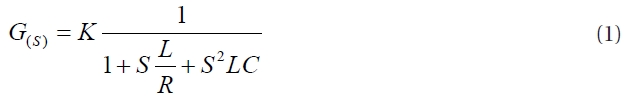
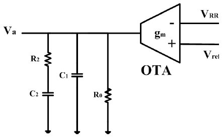
Where K, R, L, and C are the constant, resistance, inductance, and capacitance respectively, in the power stage of the boost converter. The frequency response and stability are determined directly by their poles. We can determine whether or not the converter circuit is stable by examining loop gain as a function of frequency. Figure 3 represents a compensator with OTA. The two capacitors and a resistor are used to generate pole or zero. The transfer function of the compensator is given as
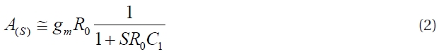
Where Ro is the output resistance and gm is the transconductance of the OTA. The loop gain depends on the multiplication of Eqs. (1) and (2). The purpose of introducing the pole in the compensator is to provide a sufficient phase margin in the loop gain. When the pole in the compensator is located on the left side of the poles of Eq. (1), the phase margin is usually increasing, and more stability can be obtained.
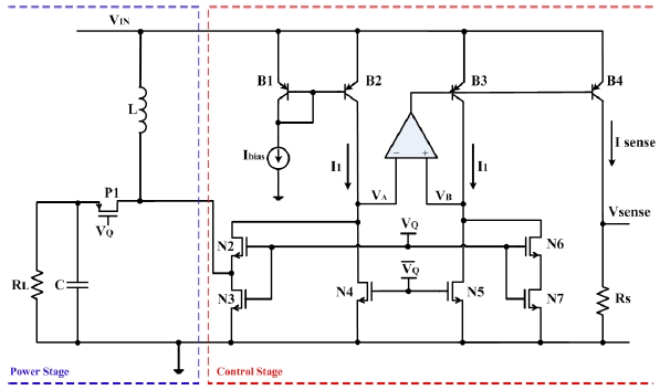
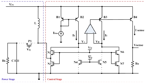
The current sensor in Fig. 4 is realized by the power PMOS transistor N3 and SENSEFET N7. The transistors P1 and N2 are the switches for the ON-OFF states. The matching of transistors N3 and N7 depends on process parameters such as mobility μ, oxide capacitance Cox and threshold voltage VT. An op-amp is used as a voltage mirror to enforce the same voltages at voltage VA and voltage VB. Any change in VA will force a similar change in VB, due to the virtual short-circuit provided by the op-amp. Thus, the drain-source voltage VDS of transistor N3 is almost identical to the drain-source voltage VDS of transistor N7. However, the transistors N3 and N7 are scaled so that the power transistor N3, on the output side of the circuit, has an aspect ratio of 500:1, which is much greater than that of the transistor N7 on the sensing side. As a result, the current, Is, on the sensing side is much smaller than the current, Io, on the output side.
The output-sensing current, Isense, which passes through the resistor, Rsense, is the difference between the sensing current, IS, flowing through the transistor N7 and the current, I2, flowing through the small biasing current source. For small biasing current I2 ≪ IS, the current, Isence, flowing through Rsense is almost proportional to the current flowing through the inductor and is much smaller than the inductor current. For the current mode DC-DC buck converter application, only the sensing-voltage,
Vsense, is needed in the control feedback loop during the on-state, and the signal from the power transistor N3 during the turn-on is sensed. Thus, the design of the amplifier is very important in this sensing circuit, as it will affect the minimum supply voltage, accuracy of the sensing voltage, and stability of the entire sensing circuitry.
During the ON period represented in Fig. 5, the sensing FET N7 and power FET N3 of Fig. 4 are turned on by setting VQ high,while N4 and N5 are turned off. There are small bias currents Ibias and the inductor current IL going into N3. IN3 is approximately the same as the inductor current IL because the bias current is quite small. The drain current of sensing FET N7 is IN2/K (K is the aspect ratio of N7 and N3). Thus, the current on the sensing side is much smaller than the output current, although it is linearly proportional to the output current. During the OFF period of the sensing circuit, N2, N3, N6, and N7 are turned off. Switches N4 and N5 are turned on, and their drain currents are the same as the bias current, Ibias. As the sensed inductor current is scaled down, the power loss in the sensing circuit is significantly reduced.The accuracy of the sensed inductor current depends on the current mirror of transistors N3 and N7 in Fig. 5 and the resistor, Rsense, stated in the equation. An op-amp is used as a voltage mirror such that the sensing current, Isense, is matched to the inductor current IL. The sensing signal, Vsense, is given by:
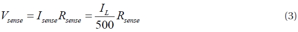
The resistor, Rsense, is used to convert the current signal to a voltage signal such that Vsense is proportional to the sensing current. As the op-amp is used to enforce the voltage, VA, to equal the voltage VB, a high-gain amplifier is needed for accurate currentsensing. This type of current-sensing circuit still has some problems, such as the offset-current, accuracy, and sensing speed. These problems are caused because the sensed current is the sum
of the scaled inductor current and the biased offset-current.
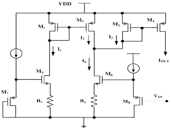
The V-I converter in Fig. 6 converts the sensing and ramp signals into currents. As shown in Fig. 1, the two signals passing through the resistor, RF, combine into a voltage which produces PWM signal. In the current-mode converter, the ramp signal is added to the sensing signal in order to eliminate sub-harmonic oscillation.
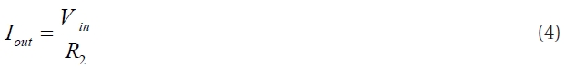
The V-I converter consists of two symmetrical sub-converters. Two sub-converters are required to eliminate the body effect of the transistor, M8, whose gate is the input voltage. The approximate output current, Iout, is given by:
The sensing voltage in Fig. 2 is given by:

Therefore, the output current, Iout, of the V-I converter is proportional to the sensing current and the ratio of resistors:
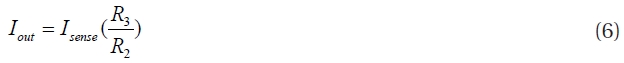
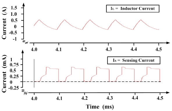
Figure 7 shows the sensing and inductor currents at input voltage of 3 V for the case of duty ratio 0.5 and frequency of 10 kHz. The inductor current IL is sensed and scaled to Isen. Isen is added to the PWM controller, which is formed by a voltage comparator, SR latch, and oscillator to generate a signal for controlling the duty cycle.
The sensing and inductor currents are approximately 0.7 mA and 0.2 A respectively. The order of the aspect ratio between the power and sense FETs in the sensing circuit is correctly adapted.
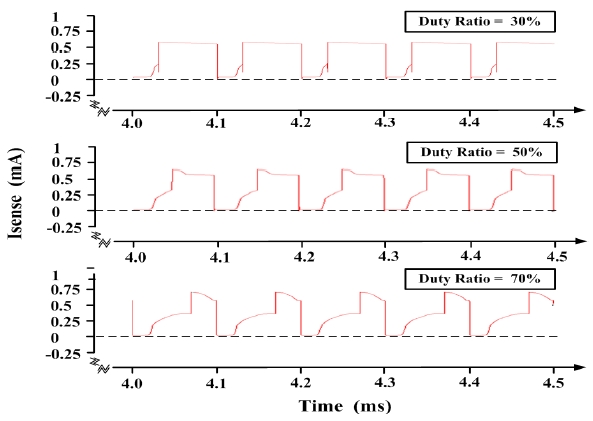
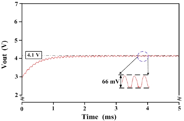
The slope of the inductor current depends on the output voltage,frequency, and inductance. The proposed current-sensing circuit is seen to accurately sense the charging of the LC accurately. The sensing current is measured by the variation of duty ratio, as shown in Fig. 8.The accurate duty ratio, excluding the time delay in the signal, is obtained. The time delay increases with higher duty ratio and is especially long in the 70% duty ratio. The time delay seems to come from the transient time for the op-amp in the current sensor to force the input voltages to be equal. The output and ripple voltages of DC-DC converter in Fig. 9 are obtained to be 4.1 V and 66 mV respectively. The output voltage is within a 5% error of the expected result. The ripple ratio is 1.5%.
A current-mode DC-DC boost converter has been designed in 0.35 μm BiCMOS process, with double-poly and four-metal layers at a switching frequency of 10 KHz. The converter is composed mainly of a power stage and a feedback network. To obtain a high performance converter, the SENSEFET method and BiCMOS technology are applied to the current-sensing circuit. In the error amplifier, cascode OTA and BiCMOS technology are used in order to yield high gain and only one dominant pole. A simulation test shows that the sensing signal is properly reflected in the inductor current by the order of the aspect ratio. The output voltage is obtained, as expected, to be 4.1 V, and the ripple ratio is controlled within 1.5%. The result indicates that the currentmode DC-DC boost converter with BiCMOS technology shows good performance in terms of current-sensing and output voltage.