Amorphous silicon thin film transistors (a-Si TFTs) are widely used for consumer electronics and have been demonstrated to be useful for use in solar cells and flexible displays. Organic TFTs (OTFTs) are of interest for applications in low-cost electronic devices such as radio-frequency identification tags, flexible displays, memory and sensors. However, the applications of these devices are limited by their low mobility and light/moisture sensitivity due to their intrinsic material properties. Transparent conducting oxide and oxide semiconductor films have been used in many applications as transparent electrode materials for flat panel display devices, touch panels, and solar cells [1].
For high performance electronic devices, low energy barriers between source-drain (S-D) electrode and semiconductor interfaces are critical to the device performances. Several approaches have been attempted to solve the problem by doping, tandem structure and a metallic interlayer. One of these effects, the modification of the electrode and organic layer interface by inserting transition metals, has received much attention in the field of solar cells [2], organic light-emitting displays [3] and OTFTs [4].
Chu et al. [4] reported that metal oxides such as molybdenum oxide (MoO3), vanadium oxide (VO3), or tungsten oxide (WO3) were introduced between the S-D and the organic semiconductor to obtain improved OTFT properties. This carrier injection layer could be expected to improve the injection efficiency by improving the contact resistance due to the metal interlayer acting as a charge injection layer and preventing diffusion of the electrode metal.
However, there was no report on the insertion of a transition metal interlayer between the S-D and oxide transistors prior to our result [5]. The main reason for no report is supposed to be the not-perfectly-matched work function between the oxide layer and the S-D, unlike in organic devices. We found that even though the matching of the work function of the transition metal is unbalanced, this method still works in terms of improving the electrical properties [5]. Here, we studied the atomic configurations at the interfaces by using X-ray photoelectron spectroscopy (XPS) to verify the presence of an intermixed state in an inkjet-printed zinc tin oxide (ZTO) TFT.
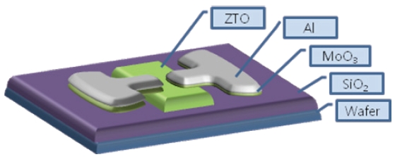
A bottom-gate and top-contact solution processed ZTO TFT was prepared. As an active layer, zinc acetate dehydrate and tin chloride were mixed in 2-ethoxyethanol to form a sol-gel solution mixture, of concentration 0.7 M with the same molar ratio of Zn and Sn, and the solution was stabilized by addition of an ethylamine. The ink-jet printing system (Ommijet Mini-100, Unijet) was used with an orifice size of 50 μm. After ink-jet of ZTO solution onto the 300 nm thick thermally grown silicon oxide gate insulator on the heavily doped silicon wafer, the films were then thermally annealed at the temperature of 500℃ for one hour. MoO3 was thermally evaporated with 1 nm of thickness and 100 nm of S-D (Al) was also deposited by thermal means. The TFT channel was 1,500 μm wide and 100 μm long. XPS analysis was performed by using a Thermo VG ESCA Sigma Probe spectrometer operated at 15 kV and 100 W with a mono-chromatic Al-Ka radiation source. The surfaces of the specimens were cleaned by Ar+ etching (2 kV, 1.8 μA) prior to recording a spectrum. The spectra were calibrated by using the C 1s peak (285 eV).
A bottom gate and top contact inkjet-printed ZTO TFT was prepared as shown in Fig. 1. We use our standard inkjet process for printing the sol-gel ZTO solution. Uniform inkjet droplet ejection was achieved by applying a 60 V pulse at a frequency of 500 Hz with a substrate temperature of 50℃ and a nozzle distance of 0.5 mm. The metallic interlayer was deposited between the oxide semiconductor and Al S-D electrodes by thermal evaporation. The structure of TFT was subjected to analysis of the interface between the layers around the MoO3 interlayer. Among the various thicknesses prepared, 0.5-1 nm thickness of the MoO3 interlayer showed better electrical properties according to our previous result [5]. Therefore, this sample was analyzed by XPS to confirm the atomic configuration of the interface between the layers of ZTO/MoO3/Al in the device.
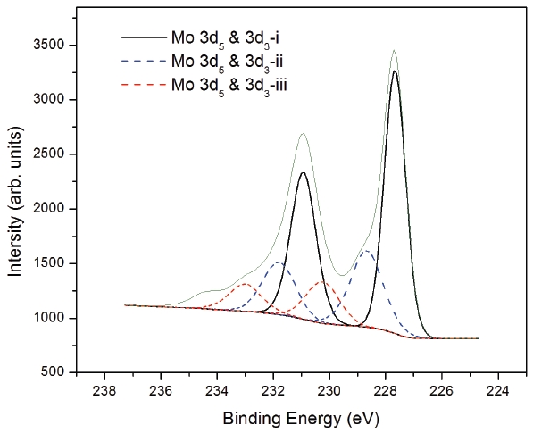
The XPS spectra were obtained after pre-cleaning the sample surface with argon plasma to remove surface contamination.The binding energies were calibrated by using the C 1s peak (254.8 eV) as a reference. Figure 2 showed the XPS spectra of the ZTO/MoO3/Al interface for Mo 3d core levels to investigate the interlayer structure. The interface result indicated by the XPS spectra is a mixed state of several different atomic configurations at the interface. There are three doublets in the spectrum,which were found after a fitting analysis with a Gaussian/Lo-rentzian mixing function. The spectrum showed three Mo 3d3 and 3d5 doublets, which indicate the presence of three types of different molybdenum oxides in different forms. We proposed that the Mo 3d5 and Mo 3d3-i correspond to the metallic interlayer of MoO3, while the Mo 3d5 and Mo 3d3-ii and the Mo 3d5 and Mo 3d3-iii represent the interface state between ZTO and
the S-D layer. The binding energies of the three molybdenum 3d3 and 3d5 doublets are 227.66 eV and 230.93 eV, 228.67 eV and 231.8 eV, and 230.24 eV and 233.00 eV, for 3d3-i, ii, and iii, respectively. These binding energies of Mo 3d core levels are a little bit lower than those of Mo 3d in spin-coated oxide semiconductor films. In the spin-coated oxide semiconductor, the binding energies of the three molybdenum 3d3 and 3d5 doublets are 227.69 eV and 231.0 eV, 229.1 eV and 232.4 eV, and 230.75 eV and 233.95 eV, respectively. From this result we postulate that the MoO3 are located in each layer in the ZTO/MoO3/Al in TFT structure. The binding energy difference for each of the three individual doublets is similar, which ensures that the results have the corresponding physical sense [6].
These values of binding energy in Mo 3d core levels are lower than those in the MoO3 crystal [7]. Furthermore, this discrepancy in binding energy between the MoO3 thin film and crystal reflects the presence of two dimensional or monomeric molybdenum oxides in the film.
The binding energy of MoO3 is shifted to a higher binding energy because of the small amount of deposition; the Mo 3d core level is shifted to a higher binding energy at the initial deposition. Two small doublets in the spectrum appear to be shifted to higher binding energy, which reflects the existence of a strong interaction of molybdenum oxo-species with ZTO and Al in a monomeric form or as two-dimensional aggregates. Even though the energy levels between the oxide and S-D electrode with the MoO3 interlayer are not matched, we found that an effective thickness still exists, due to the chemical intermixing of the MoO3 layer with Al and ZTO. The chemical reaction between MoO3 and Al occurs during the thermal evaporation of Al.
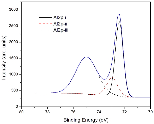
We also investigated the Al 2p core by using XPS spectra, as shown in Fig. 3. There are three different peaks found, at 72.42 eV (i), 72.98 eV (ii) and 72.96 eV (iii), in Fig. 3. These binding energies are a little bit lower than those of Al 2p in the interface of the spin oxide layer. The binding energies are located at 74.98 eV, 72.14 eV and 72.56 eV for Al on the spin-coated oxide. The binding energy shifts compared to the metallic state can be understood in terms of the difference in the bond characteristics, in which the binding energy is expected to increase from the ionic bond nature of γ-Al2O3 to the highly covalent nature ofα-Al2O3 [8].
From the three peak positions at binding energies of 72.42 eV, 72.98 eV and 72.96 eV in this interface, there are two aluminum oxo-species, that is the α-phase and γ-phase, or the high binding energy tail and metallic phase, respectively. The metallic state
is located in between the S-D electrode and the oxide semiconductor,while the other aluminum oxide compounds are in the mixed state in the MoO3 interlayer, which occurs during the thermal evaporation of Al.
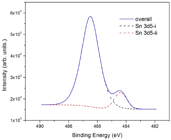
The Zn 2p3 and Sn 3d5 core shells at the interface of ATO/MoO3/Al were analyzed by XPS. Figure 4 shows the XPS data of the Sn 3d spectra at the interface between ZTO/MoO3/Al in the TFT structure. There exist two Sn 3d5 peaks: a big peak and a small peak beside it. Actually, there are two sets of Sn 3d5 and Sn 3d3 found in the XPS spectra, as in the spin-coated oxide layer. However, the intensity was quite different. In the case of the spin-coated ZTO film, the intensities of the two Sn 3d5 core shells appear to be similar. In the inkjet-printed oxide film, the intensity of the intermixing layer may be smaller than that of spin-coated one. The binding energies of the two 3d5 tin atoms are 486.48 eV and 484.38 eV. From this result we postulate that the Sn atoms in ZTO are located in the interface between ZTO/MoO3 in the TFT structure. From the peak evaluation, the 486.48 eV peak of Sn 3d5-i comes from the ZTO semiconductor layer and the 484.38 eV peak of Sn 3d5-ii comes from the MoO3 intermixed state. The full width at half maximum of Sn from the semiconductor is 1.52 and that from the intermixed state is 1.0.The binding energies of the Sn4+ and the Sn2+ peaks are assigned
as 486.5 eV and 486.25 eV in the literature [9]. For tin oxide in the ZTO system, the binding energy of the Sn2+ peak is assigned as 486.48 eV. Zn 2p3 is assigned as the 1,021.91 eV peak in the ZTO system. Because of thermal effects, the binding energies are slightly changed due to the crystalline growth of ZnO in ZTO.
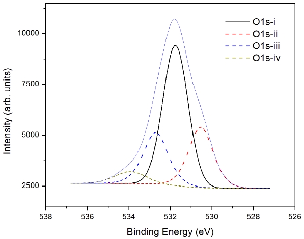
Oxygen exists in all layers in the device structure of ZTO/MoO3/Al. Therefore, precise characterization of the oxygen O 1s is not possible. The XPS measurement of oxygen in the interface in zinc-tin-oxide/MoO3/Al is shown in Fig. 5. Interestingly, four different types of oxygen can exhibit various binding energies, such as 531.76 eV (i), 530.53 eV (ii), 532.7 eV (iii) and 533.93 eV (iv). In the general ZTO system, oxygen peaks were assigned as 530.70 eV for O-, 530.15 eV for O2-, and 530.6 eV and 532.8 eV for O2-. From our analysis, the binding energy of 531.76 eV arises from the aluminum metal because the aluminum proportion made up over half of the atomic composition. The next two peaks, 530.58 eV and 532.57 eV, arise from the intermixing state of the interlayer between ZTO/MoO3/Al. The last O 1s (iv) at the binding energy of 534.03 eV showed a broad peak in the shoulder of the spectrum. Broad side peaks are the O-H bond peaks of the side tail with higher energy due to the chemisorbed oxygen. This oxygen is hard to remove because the reactive H-atoms rapidly create OH-species on an O-terminated oxide surface [10].
An XPS study was performed on the interface layer of inkjet ZTO/MoO3/Al thin layers in TFT. From XPS analysis, three Mo 3d3 and 3d5 doublets, three different Al 2p core levels, two Sn 3d5, and four different types of oxygen O 1s were found and characterized. MoO3 was found at all layers in ZTO, MoO3, and Al. This means the interface exists as a chemically intermixed state. The reason for the improvement of the electrical properties of ZTO TFT with a metallic interlayer is attributed to this chemically intermixed state, which occurs during thermal evaporation.