The micro gas sensor has the potential for use in an integrated gas detection system. A gas sensor is a device that gathers information on the chemical reaction which occurs between the sensing layer and the environmental gases. Microelectromechanical systems (MEMS) technology can potentially lead the way for the development of a micro gas sensor. The monitoring and controlling of toxic hydrogen sulphide (H2S) gas is important in laboratories and industry areas. It is used here as a process gas or is generated as a by-product. In particular, H2S is a typically badsmelling gas. The threshold concentration of it is as low as 20 ppb for human noses. Therefore, many researches are dedicated to detect the H2S gas and to develop various H2S sensing materials. Over the past decade, metal oxide thin films such as zinc oxide [1], tin oxide [2], and titanium oxide [3] have been widely investigated for their use in a H2S gas sensor application. Among the metal oxide thin films, tin oxide (SnO2) is considered as the most promising candidate for a gas sensor application. However, tin oxide materials require high operating temperatures. They also have low sensitivity. A gas sensor’s sensitivity, selectivity, and response time can be improved by adding some catalysts to the SnO2 material. Catalysts such as Pt, Au, Pd, or Ag are often added to improve the sensitivity and the selectivity [4].
The sensing mechanism in metal oxide gas sensors relies on the surface reaction of the metal oxide film [5-7]. As the operating temperature increases, molecular oxygen is absorbed into the metal oxide film. It then, accepts electrons from the surface of the metal oxide grains. At the same time, the surface of the thin film is filled with positively-charged donor ions. An electric field is formed between the positively charged donor ions and the negatively charged oxygen ions [5,8]. More the number of oxygen ions present on the surface, higher the potential barrier. Therefore, the conductivity of the thin film is lower [8]. In this state, the thin film’s surface is exposed to the reducing gas. The electrons trapped in the molecular oxygen are introduced to the surface of the thin film. This increases the conductivity of the thin film. Therefore, the surface morphology of the thin film is a critical factor affecting the sensitivity of the gas sensor [9].
Researchers have extensively studied the sensor materials based on SnO2 with CuO as catalysts using sintered pastes, thick and thin
film structures with mixed SnO2-CuO powders, SnO2-Cu bilayers and SnO2-CuO heterostructures, and chemically fixed CuO on SnO2 films [10-14]. The results of these studies show that SnO2-CuO composite thin films exhibit extraordinary H2S sensing characteristics. Their enhanced performance is due to the formation of a p-n junction between p-type CuO and n-type SnO2. Strong affinity between CuO and H2S, disrupts the p-n junction [10,11,15,16]. The H2S sensing properties of SnO2 films with catalysts are strongly dependent on the film preparation process [17-20].
This paper proposes a multi-layer thin film composed of SnO2 and CuO for H2S sensing. The sensing film with one layer is prepared by a deposition in an alternating sequence of Sn and Cu in this paper. A multi-layer sensing film was also formed through several depositions of Sn/Cu, although the entire thickness of
the film was nearly same as that of a one-layer film. Finally, an injective-type measurement system measures the H2S sensing characteristics of the SnO2-CuO multi-layer thin film.
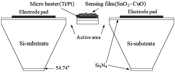
Figure 1 shows a cross-sectional view of the micro gas sensor element. The sensor was composed of a silicon diaphragm, a platinum heater to elevate the operating temperature, a SnO2-CuO sensing layer for H2S sensing, and electrode pads to measure the changes in the sensing layer’s. The sensor size and its active area were 2 mm × 2 mm and 240 μm × 240 μm, respectively. The thickness of the membrane and the platinum heater layer were 10 μm and 200 nm, respectively. For thermal isolation, the active area was isolated. It was located around the periphery of the active area.
Figure 2 shows the simplified steps for the fabrication of a micro gas sensor. The substrate used in this experiment was a 4-inch, p-type (100), double-sided polished silicon wafer with a thickness of about 300 μm. The fabrication of the sensor element was as follows: Initially, the substrate was cleaned using a piranha solution. Then RCA was cleaned and rinsed in de-ionized water. After RCA cleaning, native oxide of silicon wafer was eliminated by dipping a wafer into a 6:1 buffered oxide etcher (BOE). For silicon wet etching, a silicon nitride with a thickness of about 1600 A was deposited by a low-pressure chemical vapor deposition system (LPCVD). To define a silicon membrane, the back of the substrate was etched in to a 30 wt% potassium hydroxide solution (KOH) for 4 hrs at 80℃. This was done after photolithography and silicon nitride etching (Fig. 2(a)). Next, a silicon nitride was etched using a reactive ion etcher (RIE). To define the lift-off photolithography pattern for a micro heater with a width of 5 μm, AZ5214E from Clariant was spin-coated to about 1.2 μm onto the front of the substrate. The photoresist was then, exposed and developed. Next, 100-A-thick Ti and 2000-A-thick Pt materials were defined using e-beam evaporation and the lift-off method. Before the deposition of the heater and electrode pad materials, the substrate was treated with oxygen plasma at 60℃, 100 W for 2 minutes. This was done to improve adhesion and remove photoresist residues. Next, Ti/Pt micro heater and electrode pads were annealed for 30 minutes at 600℃ in N2 ambient (Fig. 2(b)). To passivate the micro heater and the electrode pad, a 5000 A thick silicon dioxide layer was deposited on the front of the substrate, as a protection layer, by the plasma-enhanced chemical vapor deposition system (PECVD). Contact pads were continuously opened after photolithography and silicon dioxide etching, using a contact mask
aligner and a reactive ion etcher (RIE), respectively (Fig. 2(c)). In order to fabricate the silicon bridge-type membrane, which is highly effective for the thermal isolation of the active area, the upper side of the silicon was etched by RIE (Fig. 2(d)). The thickness of the bridged membrane was about 10 μm. The size of the active area was 240 μm × 240 μm. Finally, a Sn/Cu based multilayer sensing film was prepared by electron beam evaporation by metal shadow masking.
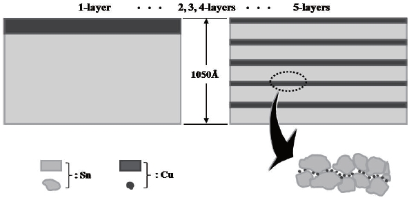
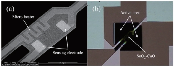
Five samples were prepared (see Fig. 3). A one-layer film was prepared by alternating the deposition of Sn and Cu. Once Sn was deposited on the sensing area, Cu was deposited as a catalyst on the Sn film. The thickness of Sn was about 1,000 A. The thickness of the catalytic Cu was around 50 A. A five-layer film was formed by five separate depositions of Sn/Cu film, each with a thickness of about 210 A. Therefore, the thicknesses of the films were equal in all the samples at approximately 1,050 A. Two, three, and four-layer films were prepared in a similar manner. The preparation of the SnO2-CuO multi-layer sensing film was completed by the thermal oxidation of the multi-layer Sn/Cu film at 700℃ for 5 hours in O2 ambient. The fabrication of the micro gas sensor was completed by dicing the substrate. Figure 4(a) shows the SEM images of the micro heater, the sensing electrodes, and the sensing layer. Figure 4(b) shows the bridge-type membrane and the active area of the fabricated gas sensor.
4.1. Microstructure of sensing films
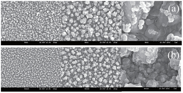
Figure 5 shows the surface morphologies of one-layer and fivelayer sensing films taken by SEM with various magnifications. The grain sizes of both the films were less than 1 μm. The grains in the five-layer sensing films were distributed more homogeneously. The grain size of the five-layer sensing film was smaller than that of the one-layer sensing film. The smaller grain is desirable for obtaining high sensitivity, as it creates a larger surface area.
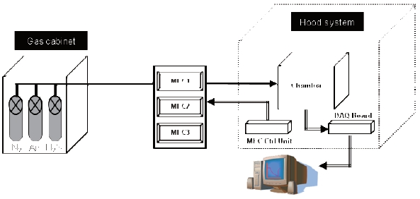
Figure 6 presents a schematic diagram for measuring the sensing properties of the fabricated H2S micro gas sensor. The sensitivities of the fabricated sensors were measured in an injectiontype reaction chamber with a volume of about 3,040 cm3. The sensor signal was collected and calculated using the data acquisition board and the LabVIEW program (National Instrument Co.).
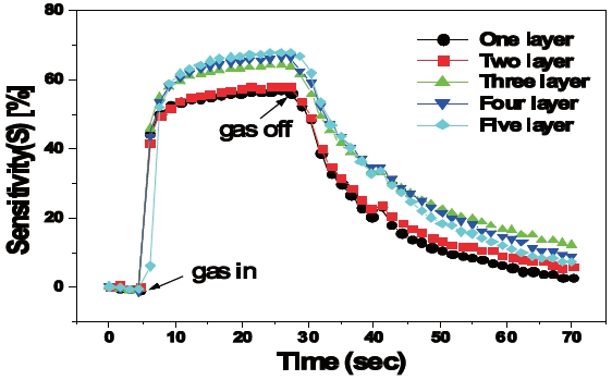
Figure 7 shows the sensitivities of a multi-layer sensing film to H2S gas with a concentration of 1 ppm at an operating temperature of about 270℃. The sensitivity, S, was defined as follows:

Where Ra and Rg are the resistances of the sensing film in fresh air and gas ambient, respectively. The sensitivity of the sensing film improved as the number of layers increased. The sensitivity of the five-layer sensing film increased to approximately 12% from that of the one-layer sensing film. It was roughly around 68%. Sensitivity improved considerably when the number of layers increased from two to three. It was observed that the size and the distribution of the grains changed sufficiently when the number of layers was more than three, as shown in Fig.5. In general, the sensitivity improved as the reaction area of the oxidizing and reducing gas increased [9]. At three seconds, regardless of the number of layers the response time of the fabricated sensors was almost equal. In our additional experiments, sensitivity of the sensor with more than five-layers was saturated although the grain size and distribution were smaller and more uniform, respectively. We therefore plan to carry out X-ray photoelectron spectroscopy (XPS), X-ray diffraction (XRD), Raman and infrared (IR) measurements to determine microstructures of layered thin films. We will then, introduce the response regarding the H2S gas sensing properties in our next paper.
This study proposed the H2S micro gas sensor which was based on a SnO2-CuO multi-layer thin film prepared by electron beam evaporation and thermal oxidation. It was found out that the sensitivity of the sensing film improved as the number of layers of film increased, while the thicknesses of films were equal at 1,050 A. The sensitivity of the five-layer sensing film for 1 ppm H2S gas was about 68% with a response time of 3 seconds. This was roughly 12% more than that of the one-layer sensing film. Therefore, alternate deposition of a SnO2-CuO sensing layer is an effective solution for H2S gas sensing.