Oxide-based thin-film transistors (oxide TFTs) such as amorphous indium- gallium zinc oxide (a-IGZO), zinc indium oxide (ZIO), zinc tin oxide (ZTO) have shown excellent electri-cal properties, including a high mobility and an excellent on/off current ratio. Especially, a-IGZO TFTs have been recognized as a very promising alternative to display backplanes of active matrix organic light emitting diodes (AMOLEDs) and thin-film transistor liquid crystal displays (TFT-LCDs) [1,2]. For practical applications, it was important to have the bias independent reliability and a number of groups have studied the stability of a-IGZO TFTs [3-7]. Particularly, the hump characteristics were considered as one of the critical issues during the operation in TFT displays affecting pixel brightness [8]. It has been reported that the stability of oxide TFTs are influenced by the absorption/desorption of gas molecules from ambient atmosphere which can be prevented by forming the passivation/capping layer on the exposed back-channel surface.
According to Ref. [9] of Huang et al, the absorption of H2O molecules in the IGZO back channel can cause a hump in the transfer curve, which can be suppressed by the passivation layer.Even in some devices with passivation layer, however, the hump had been observed. In Ref. [10] of Tsai et al, the positive bias stress-induced hump was reported in N2O plasma treated IGZO TFTs with SiOx capping layer where the hump was not observed in untreated device with the same capping layer. Although several studies have previously introduced the hump characteristics in ZnO-based TFTs, the detailed investigation on the origin of the hump has not been clarified yet.
In this work, we analyzed the anomalous hump after the elec-trical stress in a-IGZO TFTs with the bottom gate structure.
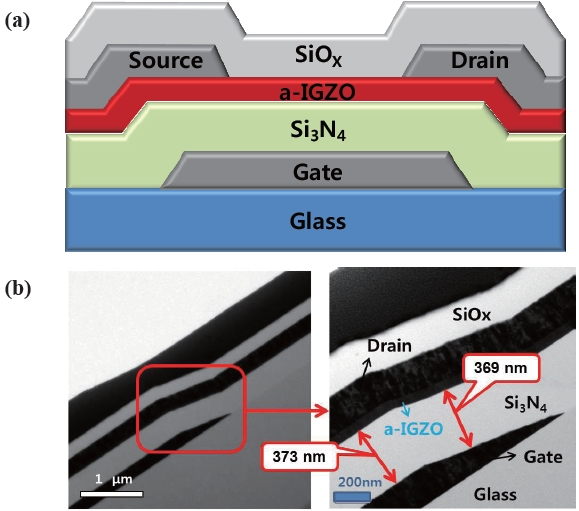
The bottom gate staggered a-IGZO TFTs were produced on glass substrate. Devices were fabricated as follows: First, sputter-deposited Molybdenum (Mo) was patterned on glass substrates to form the gate. Then, 400 nm thick Si3N4 gate insulator film was deposited by plasma-enhanced chemical vapor deposition (PECVD). Next, 70 nm thick amorphous indium gallium zinc oxide (a-IGZO) layer was grown by radio-frequency sputtering. The Mo was formed by dc-sputtering as the source and drain electrodes. After forming the source and drain on device, 200 nm
thick SiOx was deposited as a passivation layer by PECVD. Finally, the sample was annealed in O2 atmosphere at 300℃. The cross-sectional schematic and the transmission electron microscopy (TEM) image of the device are shown in Fig. 1(a) and (b), respec-tively.
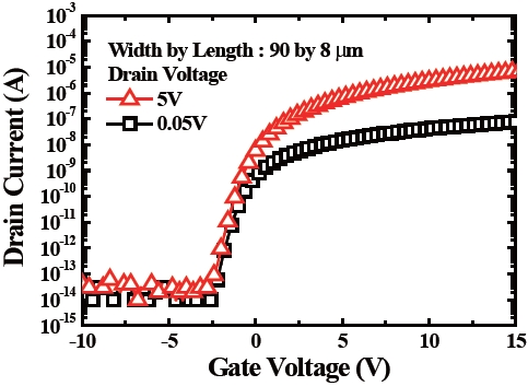
The TFT dimension used for this study was 90 by 8 μm2 (
The transfer characteristics of a-IGZO TFTs are shown in Fig. 2 and the inset shows the schematic cross section of the device.The threshold voltage (
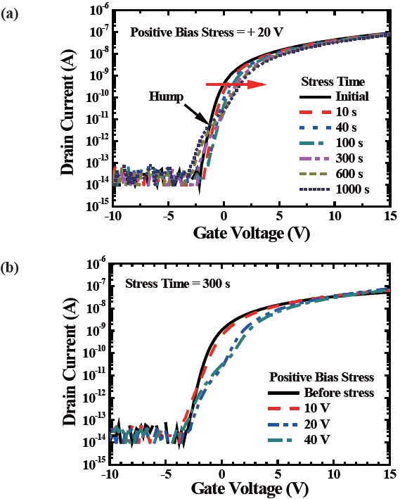
Figure 3(a) shows the transfer characteristics of a-IGZO TFTs in accordance with the gate-bias stress time at a fixed drain volt-age of 0.05 V. The constant gate bias stress of 20 V was applied while the source and drain electrode was grounded. A positive shift was observed with unchanged sub-threshold slope in the beginning. The threshold voltage shift could be explained by using an electron charge trapping mechanism [4], [11]. The trapped
electrons in the interface between the active layer and the gate oxide by the positive gate bias reduced the effective applied gate voltage, which caused a positive shift in the threshold voltage. In addition, an anomalous hump also came out for the duration of bias stress over 300 s and such a transfer curve seemed to be the combination of a dominant current path and a parasitic current path. Transfer characteristics of a-IGZO TFTs under different gate bias stress are shown in Fig. 3(b). The applied constant gate bias were 10 V, 20 V and 40 V, respectively, while the source and drain electrode was grounded. The hump appeared more clearly as gate bias stress voltage increased.
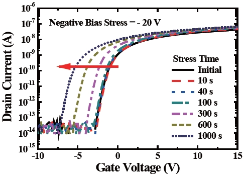
However, during negative gate bias stress, the hump was not observed. Figure 4 shows the transfer characteristics according to the constant gate bias stress of -20 V as the function of stress time. A negative shift of threshold voltage was observed with no hump and an unchanged sub-threshold slope in the transfer curve.
In poly-Si TFTs with top gate structure, the stress-induced hump was reported by the generation of the parasitic transistor as a result of the high electric field due to thinner insulator thick-ness at the active edge along the channel width direction [12]. In this works, however, the device has bottom gate structure where the gate insulator was formed after the gate patterning and so the parasitic transistor formation in the active edge was difficult. Moreover, the insulator thickness thinning at the edge was not exhibited as shown in the cross-sectional TEM image of Fig. 1(b).
It was generally accepted that free carriers in a-IGZO mainly originated from point defects (vacancies, interstitials, and antisites) in the active layer like as other ZnO-based film. There-fore, the electrical characteristics of a-IGZO TFTs were affected significantly by the density of these point de-fects, which will be determined by the process and ambient. Among these point defects, it was well known that the free electrons mainly originated from oxygen vacancies, the thermally excited oxygen atoms leaving free carriers at sites [13-15]. While these intrinsic oxygen vacancies were stable, there were also metastable point defects consisting of mobile positively charged zinc interstitial ions. The migration barrier of the zinc interstitial was so low that the zinc interstitials were mobile below room temperature [16]. The zinc interstitials were often referred to in the atomic defect model for Schottky barrier at the grain boundary in polycrystalline ZnO-base material due to their charge and mobile characteristics [17-19]. In the bottom gate a-IGZO, it was possible during the posi-tive gate bias stress, that the positively charged zinc interstitials would be accumulated at the top side of the channel layer by the field-induced migration and lower the body potential accelerat-ing the sub-channel formation. This means that the a-IGZO TFT with the bottom-gate structure had two parallel current paths under the constant gate bias stress. One was the main path through the accumulation layer induced by the gate voltage and the other was the parasitic path by the mobile zinc interstitials at the top side of the channel layer. Moreover, considering the electron trapping occurred under the gate in the positive gate bias stress as mentioned before, the sub-channel can turn on earlier. During the negative bias stress, the mobile zinc intersti-tial moved toward the gate and could not affect the hump.
Therefore, the transfer characteristics of a-IGZO TFT might be improved without humps through the process adjustment by which the formation of mobile zinc interstitial could be sup-pressed.
In this study, the anomalous hump in a-IGZO TFTs with the bottom-gate structure was investigated under constant positive bias stress and negative bias stress. During the constant positive bias stress, the anomalous hump was observed in the trans-fer curve, which seemed to be the combination of a dominant current path and a parasitic current path. However, the hump was not observed under the negative bias stress. The positively charged mobile zinc interstitial ions were accumulated near the top side of the active layer by the field-induced migration under the positive gate bias stress. Then, those lower the body potential and accelerate sub-channel formation at the top side of the a-IGZO active layer.