Nowadays, Zinc Oxide (ZnO) thin films are widely used in various applications, such as optoelectronic devices, including display devices and solar cells. ZnO has a wide direct band gap (Eg =3.37 eV) and its exaction binding energy is higher (60 meV) than that of GaN (25 meV). ZnO thin films have a hexagonal (wurtzite) crystal structure with a = 3.25 Å, c = 5.12 Å and their Hall mobility is 200 cm2/(V·s) at room temperature. Also, the high radiation resistance of ZnO thin films makes them suitable for sensors, aerospace devices and nuclear applications [1-3]. In the fabrication of optoelectronic devices, ZnO thin films have to undergo an etching process, a critical step in making a pattern. Conventional wet etching shows an isotropic etching profile. However, as the size of the device features becomes smaller, wet etching becomes less and less suitable, and is particularly unsuitable for nano scale line widths due to the isotropic properties and this kind of etching displays. On the other hand, dry etching is distinguished by its anisotropic profile. As a result, the dry etching process is suitable for micro feature size line widths and high aspect ratios.
In this study, ZnO thin films were etched with N2/Cl2/Ar gas in inductivity coupled plasma (ICP). The characteristics of etching on ZnO thin films were investigated in terms of etch rate and selectivity with various processing parameters, including the gas mixing ratio, RF power, bias power, and process pressure. The plasmas were characterized using optical emission spectroscopy (OES) analysis. The chemical binding states in the surface of the etched ZnO thin films were investigated with X-ray photoelectron spectroscopy (XPS).
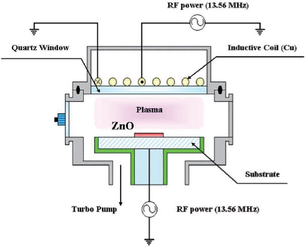
The ZnO thin films used in this work were deposited on the 6" Si substrates by atomic layer chemical vapor deposition [4]. The final thickness of the ZnO thin films was about 200 nm. The etching experiments were performed in a planar ICP system whose schematic is shown in Fig. 1. The ICP system consists of a chamber, electrodes, gas supply, mass flow controller and turbo molecular pump. We investigated the etch rate of the ZnO thin films under various experimental conditions. A process variables
[Table 1.] Process conditions.
Process conditions.
was fixing the gas mixing ratio at Cl2/Ar (16:4 sccm). The gas mixing ratio was varied to find how it influenced the etching. In addition,plasma etching of ZnO films was investigated by changing the etching parameters included in Table 1. The additive N2 gas flow rate was increased from 5 sccm to 20 sccm in steps of 5 sccm. The base condition of the experiment consists of four basic parameters: a flow rate of 20 sccm, RF power of 800 W, bias power of 400 W, and process pressure of 2 Pa. The experiments were performed by changing a specific parameter while maintaining the other parameters in their base condition. A surface profiler (α-step 500, KLA Tencor) was used to determine the etch rate of the ZnO thin films. Changes to the chemical composition in the chamber were analyzed with an OES (SC TECH, PCM 420). The chemical reactions on the surface of the etched ZnO thin films, were determined by XPS (SIGMA PROBE, Thermo VG) with Al Kα (1,486.6 eV) radiation at 300 W. The XPS equipment consisted of a micro focused monochromatic source and electron gun with a power of 15 kV. All XPS samples consisted of ZnO thin film with a size of 1 × 1 cm2.
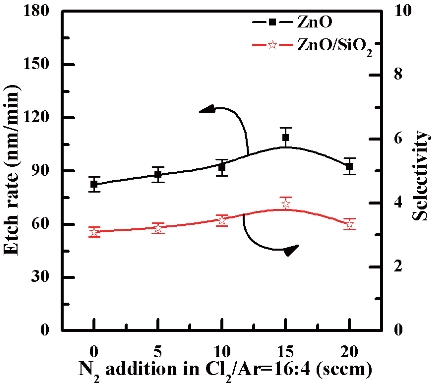
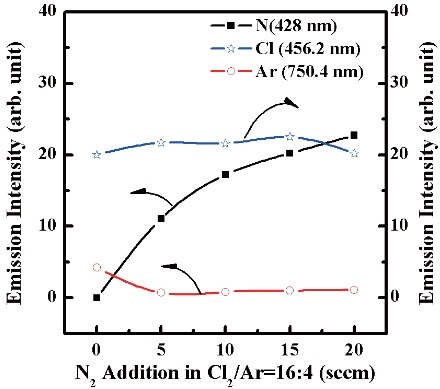
For the characterization of ZnO thin film in an ICP system, the plasma etching of ZnO thin film and SiO2 were systematically investigated in regards to the N2/C12/Ar gas mixing ratio. Figure 2 shows the etch rate on the ZnO thin film and the selectivity of the ZnO to SiO2 as a function of the N2 content in the Cl2/Ar plasma. The etch rate of the ZnO thin film at an N2 flow rate of 0 sccm was 82.5 nm/min and the selectivity was 3.21. As the N2 content was increased up to 15 sccm, the etch rate and selectivity of the ZnO thin film increased to 108.5 nm/min and, 3.98, respectively. On the contrary, the etch rate of the ZnO thin film was decreased to 92.7 nm/min and the selectivity to 3.34 when the N2 flow rate set to 20 sccm. The chemical reactions on the surface of the etched ZnO thin film in the Cl2/Ar plasma included the creation of ZnxCly from the Cl radicals [4,5]. The N atom has a very low
electron affinity (7 KJ/mol) and lighter atomic weight (14.0067 g·mol-1) compared to Ar (39.948 g·mol-1). Furthermore, the ionized N atoms would be expected to play the role of a physical etch through the bombardment of ions such as Ar ions. The ion bombardment by the N ions supported the chemical reaction of Cl2 in conjunction with the Ar ion by breaking the oxide bonds [5-7] In addition, we assume that reaction a product exists in the form of NxOy, and ZnxNy [8-12], even though the electron affinity of N is very low. In this paper our focus is on the role of the additive N2 gas. In our opinion, the results of experiments performed by varying the etch rate suggests that the N2 gas induced both physical etching and chemical reactions on the surface of the ZnO thin films [13,14]. In our opinion, the increasing etching rate in N2/Cl2/Ar plasma at higher N2 flow rates may be explained by two factors. The first factor is connected with the N2 gas assisting the physical Ar sputtering of both the main material, the ZnO film in this case, and the surface layer of the reaction products. The contribution to physical sputtering in the etching process is confirmed by the fact that the etching rate using a N2 mixed gas chemistry is higher than in Cl2/Ar gas chemistry. The second factor is connected with the acceleration of chemical interaction due to the increasing reaction probability and destruction of Zn-O bonds. The higher concentration of reactive Cl species in the N2 content plasma causes the etch rate to increase. The ZnO thin film etch rate is strongly dependent on the Cl radical concentration, due to the higher vapor pressure of the metal chlorides in Zn-Cl. However, when the N2 flow rate was 20 sccm, the etch rate decreased because the probability of reactions such as N-O or Zn-O are increased more than the Zn-Cl reaction.
Figure 3 shows the optical emission intensity of additive N2
gas flow at a fixed Cl2/Ar (16:4 sccm) ratio. These lines for Ar [750 nm], Cl [452.6 nm] and N [428 nm] are frequently used for analytical purposes including optical emission actinometrical to determine the absolute densities of active particles. For the N2/Cl2/Ar plasma, Cl emission intensity increased with increasing N2 gas flow up to 15 sccm. Also the N2 emission intensity shows an increasing trend with increasing N2 content in the Cl2/Ar mixture. As a result, Fig. 2 shows the effect of N2 content on the etch rate and selectivity.
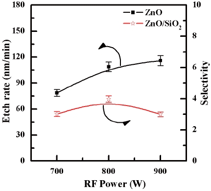
Figure 4 shows the etch rate of the ZnO thin films and the selectivity of ZnO to SiO2 as a function of the RF Power. The etch rate of the ZnO thin film increased from 78.6 nm/min to 115.9 nm/min as the RF power was increased from 700 W to 900 W. The selectivity of the ZnO to SiO2 increased from 3.0 to 3.98 as the RF power was increased from 700 W to 800 W. However, the selectivity decreased back to 3.0 at an RF power of 900 W. This implies that the RF power affects the SiO2 thin film more than the ZnO2 thin film. Generally, the etch rate increased as the RF power increased. A high RF power allows more electrons to collide with the Cl2/Ar molecules. For this reason, a high RF power enhances the dissociation rate of the injected Cl2/Ar molecules in the reaction chamber. As a result, the dissociation of the Cl2/Ar molecules and activated ions increases the plasma density. In conclusion, increases in the amount of Ar and N ions and reactive Cl2 radicals increases the etch rate by means of reactive ion etching.
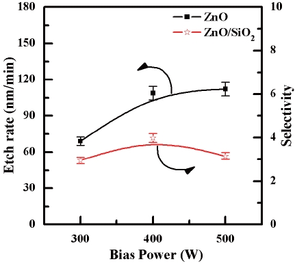
Figure 5 shows the etch rate of the ZnO thin films and selectivity of the ZnO to SiO2 as a function of the bias power. The etch rate of the ZnO thin films increased from 69 to 112.2 nm/min as the bias power increased from 300 W to 500 W. The ion bombard-
ment and the energy of the ion flux are critical factors in improving the etch rate. The physical sputtering by ion bombardments is associated with the bias power. The selectivity of the ZnO to SiO2 increased from 2.95 to 3.98 as the bias power was increased from 300 W to 400 W. The selectivity at a bias power of 500 W was decreased to 3.15. In our opinion, this phenomenon is caused by saturated ions and radicals in the reaction chamber. Further increasing the amount of ions and radicals improved the etch rate, however this also caused an increase in the pressure of the reaction chamber and in the density of the plasma. The increased chamber pressure makes the mean free path of the radicals and ions too short for a sufficient number of them to arrive at the ZnO surface. In addition, by-products after the chemical reactions remain on the surface of the film instead of being efficiently removed from the reaction chamber. The decrease of the etch rate can be attributed to factors such as the short mean free path caused by the increased pressure and the inefficient removal of by-products.
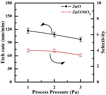
Figure 6 shows the etch rate of the ZnO thin films and selectivity of ZnO to SiO2 as a function of the process pressure. The etch rate decreased as the pressure increased. In concrete terms, the etch rate of the ZnO thin films decreased from 117.2 to 97.2 nm/min as the process pressure increased from 1 Pa to 3 Pa. The etching tendency of SiO2 is similar to that of the ZnO thin film. As a result, the selectivity remained between troughly 4 and 3.14. If the process pressure is low enough, the mean free paths of the ions and radicals is sufficiently long. In these conditions, the ions and radicals can avoid colliding with other ions and radicals until they arrive at the substrate.
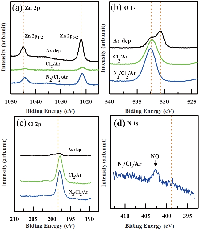
Figure 7 shows the XPS narrow scan spectra of the (a) Zn 2p, (b) O 1s (c) Cl 2p and (d) N 1s peaks of the etched ZnO thin films as a function of the gas mixing ratio. As shown in Fig. 7(a), the Zn 2p peak of the as-deposited ZnO thin films decomposes into two peaks at binding energies of 1,021.75 eV (Zn 2p3/2-O) and 1,044.95 eV (Zn 2p1/2-O). After etching, the position of the Zn 2p picks were shifted by ±0.4 eV toward a lower binding energy compared with the as-deposited sample. This chemical shift indicates that fewer Zn-Cl bonds were present in the ZnO thin film surface. This shift of the peaks brought them closer to the binding energy of metallic Zn than that of the Zn-Cl bond. According to previous reports, the shift of the peak toward a higher binding energy means that Zn-Cl bonds exist in the surface. In our opinion, the physical etching ratio is higher than the chemical etching ratio. Therefore, we believe the Ar ions destroyed the Zn-O bonds and the Cl radicals also reacted with the O atoms rather than the Zn atoms. As such, by-products such as ClxOy were removed from the ZnO thin film surface by the turbo molecular pump or the metallic Zn atoms remain until they react with the remaining O,
Cl, and N atoms. Also, we assume that Zn was bound to Cl or N at a low binding energy so that the Zn-Cl bond peak overlapps with the Zn-O peak at 1,021.5 eV. As shown in Fig. 7(b), the O peaks are shifted toward a higher binding energy. We suggest that the amount of O-O bonds was increased in the surface. This suggests that the Ar ions break the Zn-O bonds and the separated O atoms recombine with other O atoms. This phenomenon is caused by the fact that O has a higher electron affinity than Zn. The O 1s peak of the as-deposited sample was decomposed into two peaks corresponding to the Zn-O bond (530.8 eV) and the O-O bond (532.5 eV). After the Cl2/Ar plasma etching, the previous O-O bond peak was separated into two peaks corresponding to the O-O bond and O-H bond. Therefore, the intensity of the peak for the O-O bond was dramatically increased. However, the O-O peak was shifted to 531.7 eV and the other O-H peak appeared at 532.7 eV. We believe that the O-H bond peak was due to contamination of the ZnO thin film surface due to its exposure to air. Also, we assume that the additive N2 gas combined with the O atoms. For this reason, the peak of the N-O bond appeared at 531.9 eV. There is also a possibility of O-Cl bond formation, although this was not observed in this work. Figure 7(c) shows the XPS narrow scan spectra of the Cl 2p peaks of the ZnO thin films etched in Cl2/Ar and N2/Cl2/Ar plasma. As shown in Fig. 7(c), the peak positions of Cl 2p were shifted by ±0.5 eV toward a lower binding energy compared with the binding energy (198.5 eV) of the as-deposited sample and this chemical shift indicates that a chemical reaction exists on the surface of the ZnO thin films. The XPS Cl 2p peaks of the etched samples were decomposed into two peaks corresponding to the Zn-Cl bond (199.7 eV) and the HCl/H2O bond (198.3 eV). We assume that hydrogencontamination caused the HCl/H2O peak. Also, Fig. 7(d) shows a N 1s peak in N2/Cl2/Ar plasma. In the N2/Cl2/Ar gas chemistry, a weak N 1s peak appeared at 402.9 eV. This peak was identified as N-O bonds. In our opinion, the N-O bond can be explained by two factors. The first factor is Zn-O bonds being broken by ion bombardment. The second factor is the possibility of a chemical reaction between nitrogen ions and the separated oxygen ions from the Zn-O bonds. Also we expected to detect other nitrogen compound peak such as Zn3N2 and Zn(NO3)2.6H2O in the XPS narrow scan spectra of the N 1s, however we did not detect these other peaks [7-14].
We investigated etching characteristics on ZnO thin film in N2/Cl2/Ar plasmas using an inductive coupled plasma (ICP) system. It was found the additive N2 gas enhanced the etch rate.The maximum etch rate was 108.8 nm/min at an RF power of 800 W, a bias power of 400 W, a gas mixture of N2/Cl2/Ar (15:16:4 sccm) and a process pressure of 1 Pa. From the result of the XPS analysis, it was found that the Zn 2p spectra were shifted to lower binding energies and the O 1s spectra were shifted to higher binding energies after the plasma treatments. Also, the N-O peak (402.9 eV, 530.8 eV) was obtained from the XPS narrow scan spectra of the O 1s and N 1s peak. As a result, the N2 gas had the following two effects on the ZnO thin films: At a high bias power,the ion flux and ion bombardment of N ions promoted the physical etching mechanism with Ar ions. Secondly, the N2 gas resulted in chemical reactions leading to the formation of NxOy. For this reason, we suggest that the N2 gas contributed to both chemical and physical etching.