Recently, many researchers gained the interest to study transparent zinc oxide (ZnO) thin film semiconducting nanostructures. They were interested to study their potential properties and applications especially in field effect transistor (FET), light emitting diode, laser diode and other optoelectronic devices [1-5]. Owing to a direct and wide bandgap of 3.3 eV at room temperature and its ability to alter or tailor the bandgap makes ZnO to become a potential candidate for further exploration and study. Tailored materials are necessary to build many technologically important devices including field effect transistor in transparent electronics based [2-3]. Tailoring and altering the bandgap will affect the electrical behavior as well as other properties. This can be done through doping, alloying and heterostructures with some materials such as Al, Mn and Mg [6-8]. Till date, Mg is the most popular dopant material as the ionic radii of Mg2+ and Zn2+ are nearly equal and so, this resulted in a very little lattice distortion when Zn ion is replaced by Mg ion [8,9]. However, there is a difficulty of tailoring the bandgap due to the immiscibility of the different crystal structures between ZnO (wurtzite) and MgO (rocksalt) [10]. Hence, many reports have come out with lots of technique in order to deposit MgZnO thin film and overcome that problem such as metal-organic vapour phase epitaxy (MOVPE) [11], molecular beam epitaxy (MBE) [12], RF magnetron co-sputtering [13], sol-gel [14], etc. Among all the deposition techniques, it is believed that sol-gel has got certain distinct advantages in the making of alloy oxides and doping. Besides being an easy and cheap operation, low processing temperatures lead to the easiness in the kinetics control and also in the minimization of chemical interaction between the material and the container wall. It also leads to an excellent compositional control. To be more significant, it also leads to an ability to achieve atomic scale mixing of individual components [14]. The growth of MgZnO thin film at high temperature and its physical properties, the electrical properties that are to be used as high-k dielectric material, and the effect of post annealing on a thin film has been reported earlier by Kim et al., Liang et al., and Meher et al., respectively [15-17]. However, none of them have emphasized the effect of those processes on the bandgap, which more or less reflects the electrical properties of MgZnO thin film as well as other properties.
Hence, in this paper, we present the bandgap alteration of transparent ZnO thin film by using Mg dopant. Moreover, we also present the growth of MgxZn1-xO (0.0
The MgxZn1-xO (0
The starting materials that were used were zinc acetate dehydrate [Zn(CH3CO)2.2H2O], together with solvent, 2-methoxyethanol [C3H8O2], mono-ethanolamine [C2H7NO] as a stabilizer and magnesium nitrate hexahydrate [Mg(NO3)2.6H2O] as a dopant. For 0.4 M solution, with x varies from 0.0 to 0.3, the weightage of each chemical have been calculated before being mixed and stirred together in one solution respectively, as has been discussed elsewhere [1].
Before the deposition process, the solution was placed in a sonicator for about 30 minutes before being stirred and left at room temperature for 2 h. The deposition of a thin film was done in a spin coater with Ar gas at 4 mbar, 0.5 s/lit. The spin coater was programmed to rotate at 3000 rpm for 60 sec. During rotation, 10 drops sol was dropped onto the substrate. Then, each layer was pre heated at 150℃ for 10 min. Annealing process took place after the completion of all those 5 layers at 500℃ for 1 h. This process was repeated for x = 0.1, 0.2, and 0.3.
The surface morphology of the thin film has been studied by using field emission scanning electron microscopy (FESEM, ZEISS Supra 40VP). The optical properties were observed by UV-VIS Nir spectrophotometer (Varian Cary 5000) and photoluminescence (PL) (Horiba Jobin Yvon-79 DU420A-OE-325) spectrometer in order to calculate the band gap. Finally, the electrical properties of each sample were analyzed by using Keithley 2400 I-V measurement system.
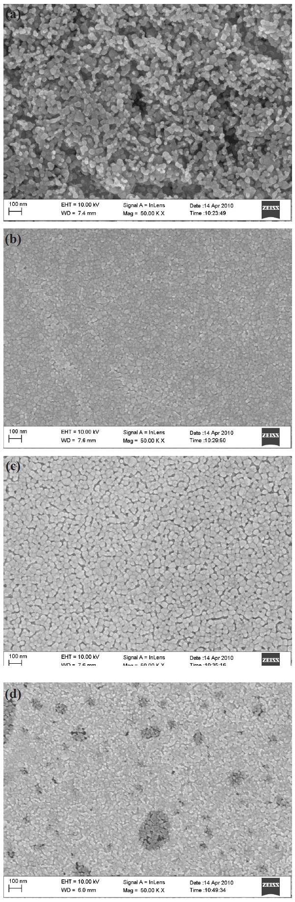
The surface morphologies of MgxZn1-xO (0.0
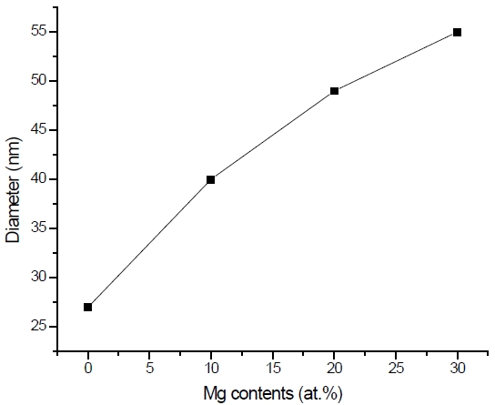
oxide can be seen with an average diameter of 20 nm. This grain size becomes bigger and the surface becomes rougher but more uniform when the atomic percentage of magnesium increased as depicted in Fig. 1(b), (c), and (d). This is due to the substitution of magnesium ion with zinc during the sol-gel process. The increment in the diameter size of MgxZn1-xO (0.0
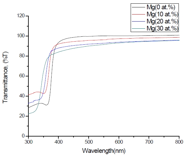
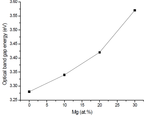
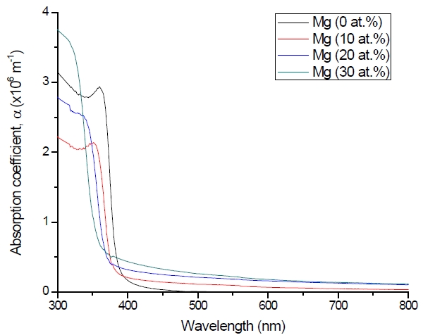
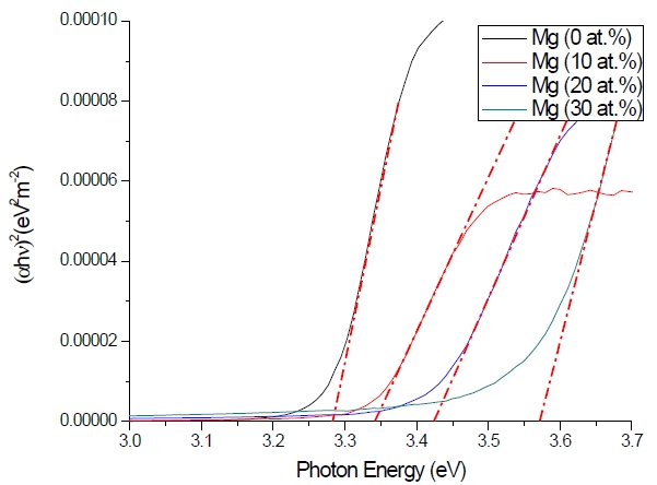
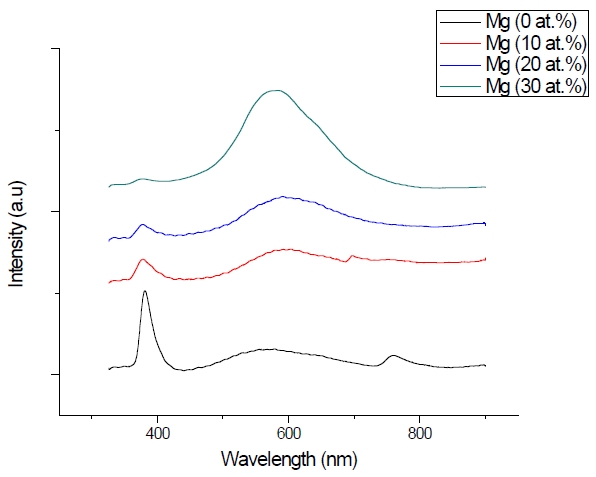
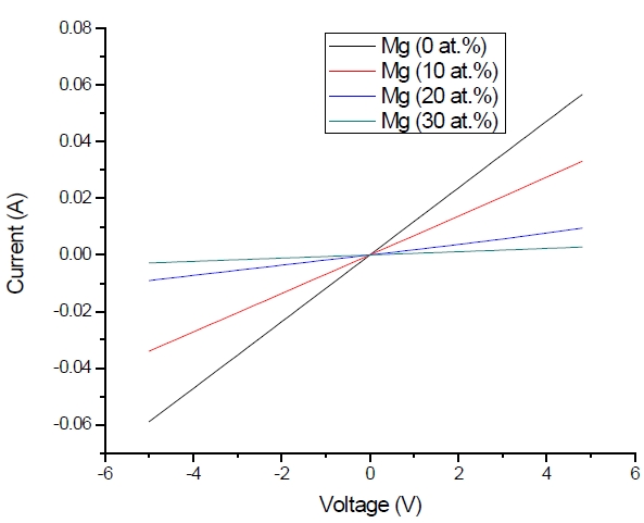
Figure 3 shows the optical transmittance spectra of MgxZn1-xO (0.0 Conversely, Fig. 4 shows the absorption coefficient, α of MgxZn1-xO (0.0 for various Mg contents. The absorption coefficient was calculated using the transmittance data, which has been presented previously. Lambert’s Law has been applied to obtain the value of absorption coefficient at a respective wavelength with the Eq.(1) as follows: where, Approximately, the bandgap alteration of the thin film can be deduced from Fig. 3. Here, it evidently shows that changes in the absorption edges are in parallel with the Mg progressed in the thin film. In order to appropriately estimate the optical bandgap, the Tauc`s plot is used, as the following equation: where, edge emission contributed to the free exciton recombination [18]. The second broad peak, also known as the green emission corresponds to the recombination of a photon generated hole with an electron in singly ionized [18]. From the first peak, the optical bandgap can be simply calculated by using the relation, where, Further investigation on electrical properties was carried out using Palladium metal contact. Fig. 8 shows the current-voltage (I-V) characteristics of MgxZn1-xO (0.0 When the four-point probe measurement took place, the reading shows an increasing value of sheet resistance with an increasing number of magnesium ions in the thin film. This is probably due to the widening of the energy bandgap with more magnesium ions to substitute the zinc oxide [16].


In summary, the physical, optical and electrical properties of MgxZnO1-x (0.0