In this study, deposition of low-dielectric constant SiOC(H) films by conventional plasma-enhanced chemical vapor deposition (PECVD) were investigated through various characterization techniques. The results show that, with an increase in the plasma power density, the relative dielectric constant (k) of the deposited films decreases whereas the refractive index increases. This is mainly due to the incorporation of organic molecules with CH3 group into the Si-OSi cage structure. It is as confirmed by FT-IR measurements in which the absorption peak at 1,129 cm-1 corresponding to Si-O-Si cage structure increases with power plasma density. Electrical characterization reveals that even after fast thermal annealing process, the leakage current density of the deposited films is in the order of 10-11 A/cm at 1.5 MV/cm. The reliability of the SiOC(H) film is also further characterized by using BTS test.
There is a continuous demand for the minimization of the pattern size and increase in the integration of the ultra large scale integration (ULSI) devices while maintaining high speed and the metal pitch also needs to be decreased below 0.13 μm. The current inter-metal dielectric (IMD) material, SiO2 is not suitable for advanced submicron devices, due to the issues of RC delay, power dissipation, and signal noise that are caused by the line stray capacitance [1]. To overcome these issues, Cu metal lines and low-k IMD material are being considered [2]. The current SiO2 IMD material has excellent physical and mechanical properties, but it is hard to reduce the signal delay time of the device due to its high dielectric constant of 3.5-4.5. Thus, extensive research work is required to obtain an IMD stack that has an effective k value below 3.0 after an integration of below 90 nm device nodes. The International Technology Roadmap for Semiconductors (ITRS) shows that research and development in the below 65 nm connection process are focused on the material that have a dielectric constant less than 2.7 [5]. One of the methods to obtain ultra low-k materials was to create a uniform porous air structure inside the low k film after post-treatment with a porogen (polymer pore generator) [6]. However, this method has some disadvantages in terms of electric leakage current characteristics and reliability after post-treatment. Recently, inter-metal insulating materials such as methyl-silsesquioxane (MSQ), hydrogen-silsesquioxane (HSQ), SiLK, SiCOH, Aurora, etc., have been investigated as low k candidates [3,4]. Among them p-SiOCH film (k < 2.4) has particularly drawn attention due to its low k value and appropriate electrical properties [7]. In this study, the hybrid SiOC(H) films were prepared by the PECVD method using trimethylsilane (TMS; SiH(CH3)3) isomer and N2O active gas. Their insulating properties are studied at different deposition conditions. The effect of the plasma power on the electrical and chemical properties of low-k SiOC(H) film was examined by using various characterization techniques.
The ultra low-k SiOC(H) films (200 and 500 nm) were prepared by a commercial PECVD (AMAT, USA) tool on 200 mm p-type (100) silicon wafers with a deposition uniformity of less than 3% by maintaining a constant distance of 7.6 mm between the shower head and the wafer. A chamber pressure of 4.5 Torr at a constant substrate temperature of 350℃ was used with TMS as the precursor in the He-diluted N2O gas environment. Active species such as TMS and N2O were utilized within the plasma power range of 0.2-2.0 W/cm2. The chemical structure of low k film was characterized by using FT-IR spectroscopy (ACCENT/QS2200M). The IR absorbance spectrum in the range of 400~4,000 cm-1 was obtained. The band structure was in the range of 900~1,250 cm-1 based on Si-O as the base matrix was analyzed. An Al/SiOC(H)/p-Si stack of a metal-insulator-silicon (MIS) structure was also fabricated to analyze the dielectric constant of the film at a driving frequency of 1 MHz. The thickness and the refractive index (RI) of the film were measured on an ellipsometry (Gaertner L116) SEM (Phillips, XL30S) and on a profilometer (P2P, KLA-Tencor), respectively. The BTS test was performed with a TaN (10 nm)/Cu (200 nm)/TaN (10 nm)/SiOC(H) (500 nm)/p-Si stack structure, in order to measure the reliability of the Cu/low-k film in the temperature range of 150℃ to 350℃ as a function of the applied voltage.
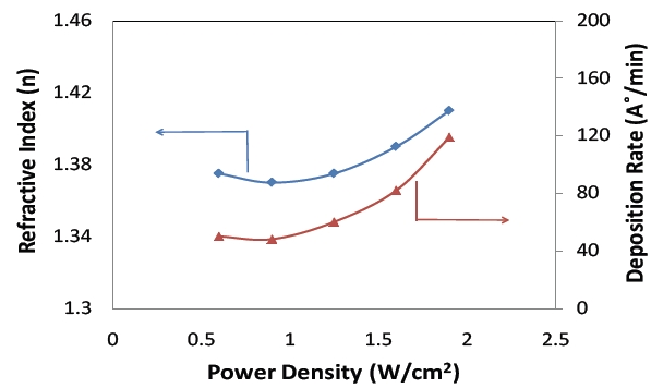
PECVD low-k SiOC(H) films were deposited on silicon wafers for various plasma power densities of the deposition system. The refractive index and the deposition rate of the SiOC(H) film were measured as a function of the plasma power density and plotted in Fig. 13 When the plasma power density was varied from 0.5 to 2 W/cm2, the deposition rate increased from 5 to 11 nm/sec whereas the refractive index increased from 1.38 to 1.41. The increase in the deposition rate with plasma power density is mainly due to the efficient generation of the radicals for the enhanced process kinetics.
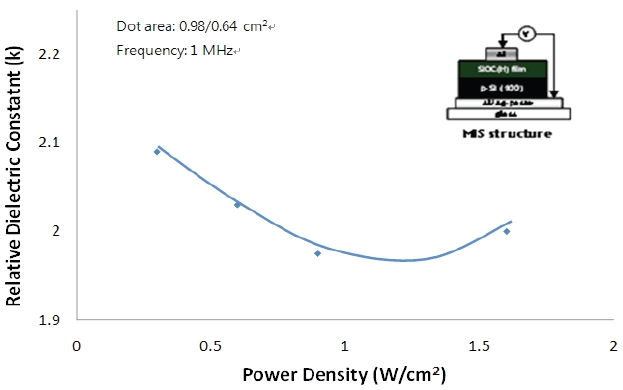
As both the refractive index and the deposition rate increases with plasma density, it may convince us to say that the film can be denser at higher plasma density. However, this may not be true always as the change in the refractive index depends on various factors such as density, composition and film bonding [8]. Thus it needs further investigation. Relative dielectric constant (k) was also measured as a function of the deposition plasma power density at a frequency of 1 MHz. The results are shown in Fig. 2.The MIS structure used
to measure the “k” value is shown in the inset of Fig. 2. As the plasma power density increased from 0.3 to 1.6 W/cm2, the value of the relative dielectric constant initially decreased and then, it reached a constant value of 1.96 from 2.1. The decrease in the k value indicates that there may be an increase in the porosity of the film with a change of plasma power density.
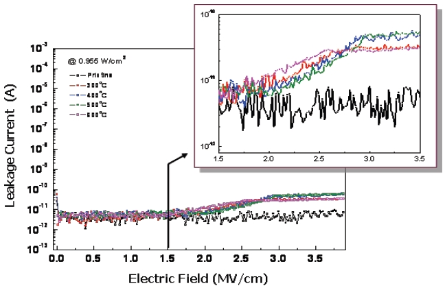
Electrical characterizations were carried out for understanding the reliability of the deposited SiOC(H) films as dielectric materials. Figure 3 shows the leakage current of the SiOC(H) film with a dielectric constant of 2.2 both before and after the FTA process. As the Fig. 3 shows, the leakage current is about 10-12 A at 1.5 MV/cm before the FTA process and the value remains the same till 1.5 MV/cm even after post-annealing at 600℃. This implies that there was no breakage in the dielectric film. Even with a further increase in the electric field to 2.0 MV/cm, the leakage current only increased slightly to 10-10 A without any breakdown of the dielectric film. These electrical properties clearly say that this low-k material is well suitable to be used as an insulator.
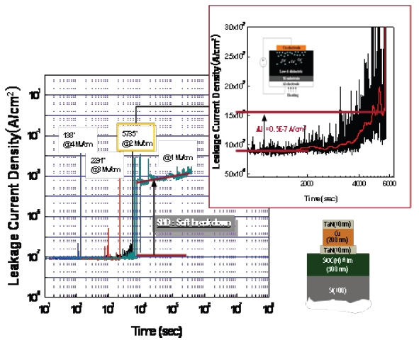
BTS tests were carried out to understand the film quality in terms of the degradation of dielectric constant as a function of time in the allowed field range of 1-4 MV/cm in the temperature range of 150℃ to 350℃ under N2 environment. Figure 4 shows the schematic diagram of the MIS structure [TaN (10 nm)/Cu(200 nm)/TaN (10 nm)/SiOC(H) (500 nm)/p-Si] which is used to measure the leakage current. The time to fail (TTF) plot for MIS
structure obtained from BTS tests is shown in Fig. 4. The TTF rate, indicates the breakdown strength and it decreases as the applied electric field is increased. As a result, the break down (BD) time, which is 138 sec under N2 environment at 175℃ with an applied field of 4 MV/cm, increases linearly as the applied field decreases.
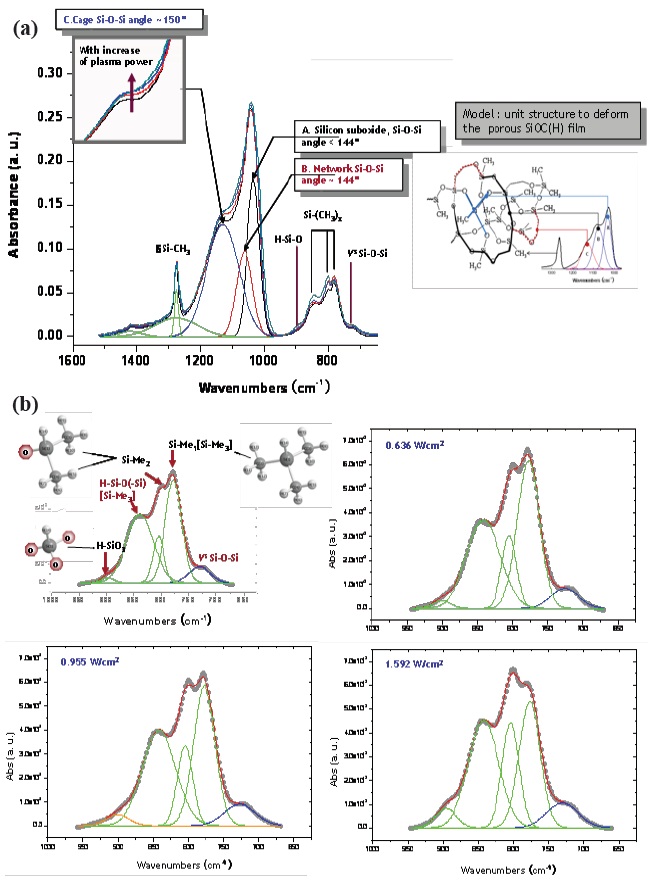
The analysis of the chemical structure of the films is critical to understand the effect of the plasma power density on the behavior of the various properties of the films such as refractive index and dielectric constant. Thus FT-IR measurements were carried out for the deposited films. Figure 5(a) shows the FT-IR absorbance spectra of ultra low-k SiOC(H) films for various plasma power densities. The detailed assignment of IR absorption peaks is given in the literature [9] and only the absorption peaks that are critical in this study are discussed here: The spectra exhibit broad band at 736-900 cm-1 is deconvolutable into five peaks. These peaks are attributed to Si-O-Si symmetric stretching (peak at 736 cm-1), Si-(CH3)x vibrations (band at 772-840 cm-1) and H-Si-O bond bending (peak at 892 cm-1).
The broad band at 900-1,250 cm-1 is associated with Si-OSi asymmetric stretching. This again can be deconvoluted into three peaks as shown in Fig. 5(b) centered at 1,129, 1,063 and 1,023 cm-1 and this result from the Si-O-Si cage like structure with a bond angle of approximately 150°, Si-O-Si network with a bond angle of 140° and Si-O-Si sub oxide structure with a bond angle of less than 140° respectively. Other contributions from C-O-C and Si-O-Si asymmetric stretching will also be overlapped with the Si-O-Si asymmetric stretching in the broad band at 1,200-1,000 cm-1. The peak at 1,273 cm-1 is attributed to the formation of SiCH3 groups in the films. Here, an increase in the plasma density increases the peak size at 1129 cm-1. This indicates the enhancement of the Si-O-Si cage structure. This enhancement along with a decrease in the dielectric constant value indicates the fact that there is a presence of a lot of organic type molecules with CH3 groups inside the Si-O matrix. This decreases the film density and consequently the molecular polarity due to the increase in porosity of the films during the formation of the Si-O cage network. Similar observations are also reported in other literatures [7,9,10]. Similarly, an increase in the refractive index with plasma power density is also due to the same factor that is, the increasing number of CH3 groups in the Si-O-Si cage as the refractive index value increases with number of carbon atoms in the Si-O matrix [8]. Thus the behavior of the refractive index, dielectric constant
and FTIR absorption spectra are consistent with each other. In addition, the peak in the range of 1,060 to 1,032 cm-1 is known to be affected by the reaction with N2O. This value is associated with the mechanical characteristics of the films with a Si-O matrix.
In this study, SiOC(H) film with a dielectric constant of less than 2.4 was deposited at optimum conditions by using plasma in a He-diluted N2 environment using TMS. The leakage current of the deposited film was about 10-12 A and this is a very suitable value for usage as an insulator. The decrease in the dielectric constant value of a film with an increase in the plasma power density is mainly due to the increase in the porosity of the film. This is due to the incorporation of organic molecules with CH3 type into the Si-O-Si cage structure. This is confirmed by the FT-IR analysis in which the absorption peak at 1,129 cm-1 was associated with the Si-O-Si cage structure and it increased with the plasma power density. This also reflected in the trend of the refractive index. It increased as the plasma power density increased due to the increased content of the carbon in the films. Thus, the results of the refractive index, dielectric constant and FT-IR are consistent with each other and they reveal that the amount of CH3 groups in the Si-O matrix mainly determines the insulating characteristics of the low -k films.