The light emitting diodes (LEDs) produce a broad range of light spectrum and intensity. They are used in a wide variety of applications such as displays, sensors, lighting, remote communications and optical links. Compared to other lighting sources, LEDs offer higher luminous efficiency, lower energy consumption, longer lifetime, improved reliability, smaller size, faster switching and wider color gamut. One of the popular LED applications is the generation of backlighting for liquid crystal display (LCD) panels. LCDs that are used for indoor and portable displays have a brightness of 100 cd/m2 whereas solid-state and organic LEDs produce a brightness of 105 cd/m2 [1].
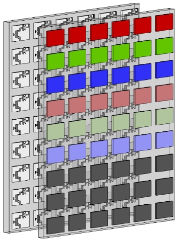
LCD panels consist of a back-side reflective surface, backlighting LEDs, a set of opaque, dotted and diffusing films for the purpose of evenly distributing, patterning, unifying and guiding the light in the proper direction, a back polarizer, a back transparent electrode is used as a glass substrate, thin-film transistor (TFT) sub-pixels, an organic liquid crystal, the red, green and blue (RGB) sub-pixel filters to generate a wide range of colors, a transparent front electrode, a front vertical polarizer and a display screen, as shown in Fig. 1. When a voltage is applied between the two transparent electrodes, the orientation of the liquid crystal molecules changes and as a result, light passes through the crystal. The intensity of light depends on the voltage that is applied between the two electrodes. The color selection is based on the switching of the sub-pixel transistors.
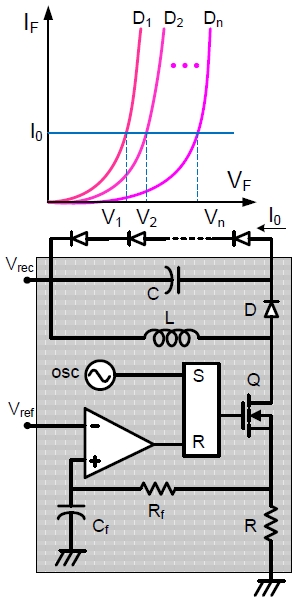
As the light of LEDs is proportional to the biasing current, all the LEDs in series configuration will have similar luminance. However, a very large voltage is required to turn ON all the LEDs. This large voltage is usually provided by a boost converter circuit,as shown in Fig. 2. In a boost converter circuit, a power transistor drives a large inductor which is switched repeatedly to alter the current through an inductor and then, to boost the voltage. This voltage is then, rectified by using a diode and a capacitor and the resulting DC voltage is applied to the series LEDs [2]. Any voltage variation at the output of the boost converter or the heating of some LEDs will change the voltage drop across all the series LEDs thereby, altering their luminance. Even a single LED failure will result in the shutdown of the whole back-light system unless some special bypass circuits are used. Due to the nonlinearity and high power loss of the boost converters at high voltage levels, global regulations require LCD monitors and televisions that use boost converters to pass through rigorous emission and power efficiency standards. Therefore, a capacitor is utilized for power factor correction and for improving the efficiency of the boost converters.
2. FUTURE DISPLAYS OF PORTABLE DEVICES
For small display screens which require less observation distance, only a few LEDs are required to provide enough back-lighting. However, in the existing LCD structures that are described earlier, more than two-thirds of the white light is generated by the backlighting unit. This gets absorbed by the opaque, dotted and diffusing films in order to manage and direct the light in a proper direction. This reduces the efficiency of the LCDs and increases the power dissipation to achieve a certain level of brightness [3]. Modification of a LCD structure and elimination of films will improve the light efficiency by three fold. Replacing color filters with controllable RGB color LEDs for direct generation of the image will also add to the further improvement in the light efficiency
Human eyes can distinguish the boundaries of objects that are as small as 50 μm. Future generations of ultra-high resolution and ultra-low power displays might utilize RGB sub-pixels which are designed by using nanowire color diodes. They are directly connected to the nanowire transistor drivers, as shown in Fig. 3. The development of III-V nanowire LEDs with Silicon nanowire
transistors on the same substrate would enable the fabrication of high resolution displays for small portable devices by using standard Silicon integrated circuit (IC) fabrication which is of low cost and requires no extra processing steps.
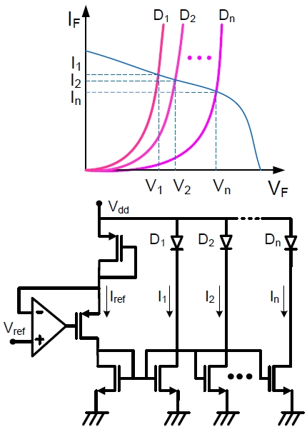
When LEDs are used as active loads in parallel, as shown in Fig. 4, they will have very similar biasing voltage and current which remains almost independent of the temperature and process variations. When the ON voltage of an LED increases due to process variation, the biasing current through that LED will decrease slightly. The biasing current of the LED will increase when the ON voltage of the LED decreases due to heating and temperature variation. Therefore, the power dissipation of all the LEDs remains relatively constant and the luminance of the LEDs is adjusted by the control voltage which is applied to the gate of transistors. In order to control the light intensity of the parallel LEDs independent from temperature variation, a bandgap reference current generator is used [4]. A fast, burst-mode pulsewidth modulation (PWM) with low ripple currents can also be used to control the desired chromaticity of the LEDs at different dimming levels [5].
3. NANOWIRE LEDs AND TRANSISTOR DRIVERS
3.1 Silicon germanium nanowire LEDs
In direct-bandgap semiconductors such as gallium arsenide, the bandgap energy occurs at the same value as the electron momentum. Therefore, all the energy of the bandgap-jump goes into the photon [6]. The quantum efficiency or the ratio of the generated photons to the electrons injected across the p-n junction is 10 percent for III-V LEDs. The Silicon crystal is an indirect bandgap. Therefore, the minimum energy in the conduction band and the maximum energy in the valence band occur at different values of electron momentum. Photons in the Silicon LEDs are generated only if crystal lattice vibrations or phonons are present. The probability of phonon occurrences is very low and so, the Silicon LEDs have quantum efficiencies in the range of 10-4-10-5 when compared to the 10-1 quantum efficiency of IIIV LEDs [7]. However, the fabrication cost of Silicon circuits is 100 times less than the fabrication cost of III-V materials and Silicon technologies offer high reliability and high levels of integration.
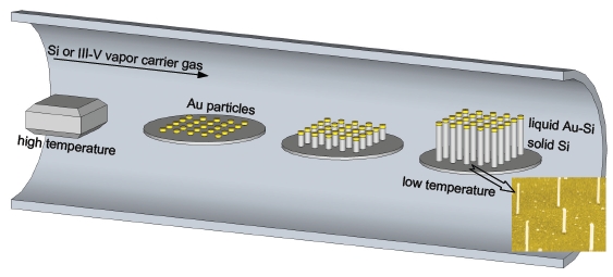
The atoms in III-V semiconductors are spaced slightly different than those in Silicon. The lattice mismatch and misalignment result in a stress in the interface layer and this makes the direct growth of the III-V materials on Silicon bulk impractical. However, at nanometer scales the III-V semiconductors can grow on top of the Silicon substrate [8], as shown in Fig. 5. Till date, IIIV nanowire LEDs are grown on Silicon substrates and they cover the entire light spectrum [9]. Application of currents to nanowire
LEDs will emit light from close to the junctions. These nanowire LEDs can form pixels of a small display in a hand-held device.
Nanowires are created using various techniques such as chemical beam epitaxy (CBE), molecular beam epitaxy (MBE), selective-area growth (SAG) and a catalyst-driven process called the vapor-liquid-solid (VLS) technique [10]. In the VLS approach, shown in Fig. 5, nanowires are grown from thin films of the metal catalyst by using several nanometers thickness sputtered on the substrate in particular the patterns created by optical or electron beam lithography. The catalyst particle is a low temperature melting material such as Au, In, Ga and Sb and is in a molten liquid form at the growth temperature. Some catalysts may contaminate the p-n materials and may even alter the carrier recombination. The III-V semiconductor growth precursor is in vapor form and so, is delivered by a high temperature and high pressure carrier gas to the catalyst particle which is on the substrate. The vapor diffuses on the molten particle and thereby, forming an alloy. After the catalyst over saturates, the precursor material precipitates out of the alloy droplet in the form of a solid nanowire that starts to grow. The diameter of the nanowire closely follows the size of the metal catalyst. The nanowire growth is epitaxial and the important features of the Silicon or Germanium crystal structure such as the orientation of the lattice planes are replicated in the nanowire. As a result, electrical contact is maintained between the nanowire and the substrate.
3.3 Nanowire transistor implementation steps
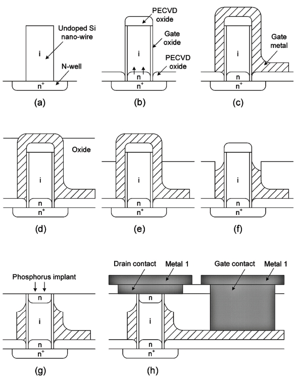
The process to create nanowire transistors [11] are outlined in Fig. 6. First, the n-well and p-well are created on a Silicon substrate. The catalyst is deposited over the n-well and p-well and a high temperature wire growth takes place. After the completion of the wire growth, the catalyst is stripped from the top of the grown wire by using a wet etch, as shown in Fig. 6(a). This
step is followed by a gate oxide growth. Anisotropic plasma enhanced chemical vapor deposition (PECVD) of SiO2 is deposited vertically on to the substrate in order to define the gate-source boundary, as shown in Fig. 6(b). The oxidation step causes phosphorus atoms from the n+ well and boron atoms from the p+ well to diffuse approximately into the Silicon wire from the substrate surface. A single work function tungsten layer is deposited as the gate metal shown in Fig. 6(c). Isotropic chemical vapor deposition (CVD) oxide is deposited and a chemical-mechanical polish (CMP) step is applied until tungsten is visible, as shown in Fig. 6(d). The PECVD oxide is recessed in order to define the depth of the drain region or drain-gate boundary, as shown in Fig. 6(e). Exposed tungsten is isotropically removed by wet etching, as shown in Fig. 6(f). A second CVD oxide layer is deposited followed by a CMP step that stops at the Silicon interface. Phosphorus and boron are implanted perpendicular to the wire end to define drain contacts for nmos and pmos transistors, as shown in Fig. 6(g). A rapid thermal annealing (RTA) step is applied to activate both phosphorus and boron implants. A CVD oxide is deposited. Aluminum contacts are formed by using a unidirectional reactive ion etch (RIE) step. An aluminum layer is deposited as the metal-1 layer, as shown in Fig. 6(h).
3.4 Characteristics of silicon nanowire transistors
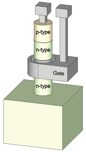
The conventional planar metal oxide field effect transistors (MOSFETs) suffer due to the short-channel effects and the decrease of the threshold voltage in the nanometer ranges [12]. In nanowire transistors, shown in Fig. 7, the distance between the source and the drain in the vertical direction does not depend on lithography but instead it is controlled by the growth time. Silicon and Germanium nanowires are grown by using the VLS technique that possesses high surface quality. Nanowire transistors provide full gate control over the channel and achieve ultralow OFF currents with minimum short channel effects [13]. For nanowires with dimensions that are less than ten layers of Silicon atoms, the electron motion becomes restricted due to the quantum confinement and so, the bandgap increases.
A three-dimensional device design study on un-doped Silicon nanowire transistors is conducted to explore the superior performance of the nanowires compared to other transistor technologies. The nmos and pmos nanowire transistors are modeled with fully depleted Spice models. When biased with VDS=0.5 V and VGS=0.5 V at the active operating region, nmos and pmos nanowire transistors have 2 μA and 0.7 μA drain currents, 14 μA/
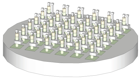
V and 8 μA/V transconductances, 400 kΩ and 1.1 MΩ output resistances, 36 THz and 25 THz unity current gain cutoff frequencies and 120 THz and 100 THz maximum frequency of oscillations, respectively. The large-signal operation of an LED driving circuit with 1 V output swing exhibits 2.2 ps delay, 5.4 ps rise time and 4.7 ps fall time while it switches at 30 GHz. A drawing of a Silicon wafer includes several integrated nanowire drivers and LEDs which are prior to metal routing are shown in Fig. 8.
The processing steps to grow nanowires on Silicon substrate are described. The vertical n-type and p-type nanowire transistors with surrounding gate structures are designed and characterized. At 0.5 V biasing voltages, nanowire transistors with minimum radius or channel width have an OFF current which is less than 1 pA, an ON current more than 1 μA, a total delay that is less than 10 ps and a transconductance gain of more than 10 μA/V. Control of nanowire LEDs with nanowire transistors will significantly lower the cost, improve the manufacturing yield and will increase the efficiency and simplicity of the small displays that are used in portable devices. The low power and fast switching characteristics of the nanowire transistor make them ideal for the realization of future displays of portable devices along with long battery lifetime.