Studies have been largely conducted on the development of thinner and lighter flexible displays by replacing glass boards to flexible boards like plastic. OLED displays have been attracted as the next generation flat panel display properly adopted to such an application. As luminescence was developed by Tang of Kodak in 1987 by using small-molecule organic thin films, technologies in OLED have been increasingly developed through various studies in industries, laboratories, and universities [1]. Advantages of a display using OLED are self-luminescence, high response time, wide viewing angle, ultra thin and high definition.These satisfy the conditions for an ideal display [2-5].
In general, although the service life of OLED requires more than 50,000 hours in TV and monitor applications, it shows a shorter life compared to PDP and LCD. Thus, studies on extending the service life of OLED have been largely conducted and a passivation technology for protecting moisture and oxygen sensitive organic materials holds sway in the success of panel businesses [6,7].
In the early passivation technology, it usually fabricated a single layer film in which a vapor deposition process using metal oxides represent excellent WVTR (Water Vapor Transmission Rate) characteristic was largely used. However, such a single layer film was difficult to satisfy the required life and it caused some defects according to process conditions. Thus, it is necessary to introduce double or multilayer passivation thin films in order to solve this problem.
OLEDs require a low penetration rate of moisture < 1×10⁻⁵ g/m2.day and complex multilayer barrier films that consists of five to six pairs of polymer and inorganic layers currently show promise for meeting these requirements [8].
Recently, a vacuum vapor deposition method has been largely used to the passivation thin film. In the case of vacuum vapor deposition method, there are a few defects on the surface or on the inside of the thin film. This is due to the particles or other elements that remained on boards. Regarding the moisture and oxygen penetrated into the thin film, the penetration can be performed through the passivation film that has lots of defects relatively [9].
In the moisture permeation characteristics, the penetration rates of the moisture are measured as different values. This is done according to the thickness and surface structure of the film in which the temperature and the relative humidity (RH) can be controlled as 10~40℃ and 35~100%, respectively.
Plasma Enhanced Chemical Vapor Deposition (PECVD) SiNx films were developed as an effective passivation layer for metallization of IC chips. Since then, they have also been applied in electronic packaging as effective barrier layers against moisture and corrosive ions. By optimizing of the deposition parameters, PECVD SiNx films can be deposited with excellent moisture resistant behaviors, step coverages and hardness [10].
In this study, an investigation for improving the degradation of OLED was performed through applying an in-situ method to OLEDs as a passivation thin film in a system. Moreover, a SiNx and SiO2 inorganic thin film vapor deposition method was developed by using the PECVD method that can apply a vapor deposition process at room temperature. A method that applies the developed method to a flexible display as a passivation layer for OLEDs was also proposed.
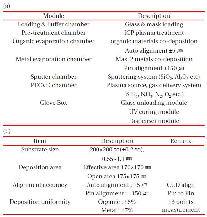
A cluster system for implementing an in-situ passivation experiment consists of a few hardware modules such as Transport Module (TM), Load Lock Module (LL), Pre-Treatment Module (PT), Organic Module (OC), Metal Module (MC), Sputter Module (SP), and Glove Box (GB). The Transport Module was configured by using a robot. It processes the glasses in the Transport Chamber and a robot arm was used to move glasses or masks in several Modules that are attached to the Transport Chamber. The Load Lock Module was a buffer space for glasses and masks and was moved to each module by using the Transport Module. The Organic Module played a role in applying a vapor deposition process and this uses the organic materials in effusion cells, to boards through a thermal evaporation method.
In order to link the PECVD chamber to the cluster system,vacuum and moving sensors were installed. Moreover, configuration works for transmitting and receiving 32 signals determined in the I/O list including glass loading (unloading) position movement, presence of chamber glasses, presence of chamber masks, state of processing a chamber process, and so on were also performed. In the system, a semi- or full-automatic process was configured for the board with a size of 200×200 mm by simultaneously installing five glasses and masks to the Load Lock. Organic vapor deposition and CVD methods were applied to organic and inorganic thin films in organic and PECVD chambers respectively. This was done for processing the in-situ passivation in a system without any exposures to the air. A total of 10 gases, SiH4, NH3, NF3, N2O, CH4, N2, H2, He, Ar, and O2 were applied to the system through a mass flow controller (MFC) as a source gas

Cluster system feature for in-situ passivation (a) Cluster system feature for in-situ passivation and (b) Cluster System for in-situ passivation.
in the PECVD system. The pipe system used in transmitting reaction gases was made of stainless steel 304 and this represents a strong anti-corrosion characteristic. The reagent gases used in the vapor deposition process of SiNx and SiO2 were SiH4, NH3, N2, and O2 with 99.999 % purity. Moreover, there was no purification process for these gases. Table 1 shows the characteristics of the in-situ passivation cluster system.
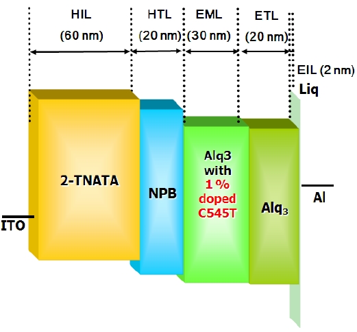
In order to fabricate OLED, glass boards were put in an OLED vapor deposition system while a vacuum state is maintained. Then, HIL (Hole Injection Layer), HTL (Hole Transport Layer), EML (Emission Layer), ETL (Electron Transport Layer), and cathode were continuously evaporated. Glasses with a size of 25×25 mm evaporated by ITO (Indium Tin Oxide) with a thickness of 150 nm were used as boards in which the organic materials used in this process were a type of luminous materials. They are given
by Alq3 metal complexes which are known as a representative host material [11]. Moreover, a luminous layer was formed by dopping a 1% C545T dopant to the host for the improvement of the luminous efficiency and element stability [12]. NPB that represents a fast transfer rate of holes and an easy formation of boundaries contacted to a luminous layer was used as a hole transfer layer [13]. In the front section of the hole transfer layer, an ITO anode, which is an inorganic metal represents high glass transition temperature and excellent boundary characteristics, and 2-TNATA. It shows excellent boundary characteristics to the hole transfer layer [14]. The evaporation thicknesses in each organic layer were determined as 2-TNATA 60 nm, NPB 20 nm, Alq3:C545T 30 nm, and Alq3 20 nm. Moreover, Liq with a thickness of 2 nm was evaporated as an electron injection layer after completing a multilayer in organic matters. Additionally, for fabricating OLED, Al with a thickness of 150 nm was evaporated as a cathode. Figure 1 shows the cross section of the fabricated element structured by using ITO (anode) / 2-TNATA / NPB /Alq3:C545T (1%) / Alq3 / Liq / Al(cathode).
In the case of an evaporation condition for organic matters, the thickness controller by Inficon was used to maintain its evaporation rate of 1 Å/sec. In the case of a cathode made of Al, the evaporation rate was determined as 5 Å/sec and the evaporation speed was measured by using quartz crystal sensors. The performance of the fabricated OLEDs was measured by using the current density-voltage-luminance (J-V-L) measurement system with Konica Minolta CS1000, Keithley 100.
The reagent gases of SiH4 20 sccm, NH3 10 sccm, and N2 90 sccm were used to perform the SiNx thin film evaporation with a thickness of 500 nm. Moreover, for obtaining the SiO2 thin film with a thickness of 500 nm, the evaporation processes were applied for 500 sec at a process pressure of 20 mTorr with an RF
power of 200 W and for 175 sec at a process pressure of 20 mTorr with a flow rate of SiH4 30 sccm and O2 60 sccm.
A passivation layer should present itself flexible for fabricating OLED by using in-situ passivation and the passivation layer is to be evaporated at a low temperature as organic matters usually have low glass transition temperature. The characteristics of such a passivation layer can be determined as follows. First, it should protect the diffusion of unwanted impurities as moisture and oxygen show difficulty in diffusion through thin films. Second, it should not be easily broken and generate cracks from external stresses. Third, it should cover the internal layer very evenly and it should present an evaporation work with very small defects like pinholes.
A chemical evaporation method using plasma generates high responsive radicals and ions by dissolving reagent gases by means of electrons. They have a high kinetic energy level due to electric or magnetic fields. This can satisfy such characteristics and makes it possible to fabricate various types of thin films at room temperature. Thus, this method was used in this experiment.
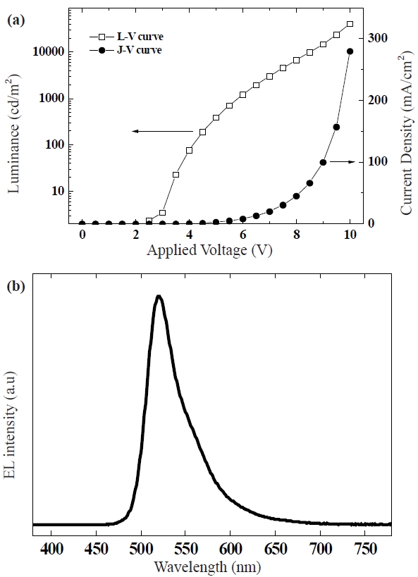
Figure 2 shows the J-V-L (Current density-Voltage-Luminance) characteristics of the fabricated OLED. As a result, the element was a green emitting OLED and the maximum emission and power efficiencies exhibited were 14.24 cd/A and 11.8 lm/W, re-
spectively.
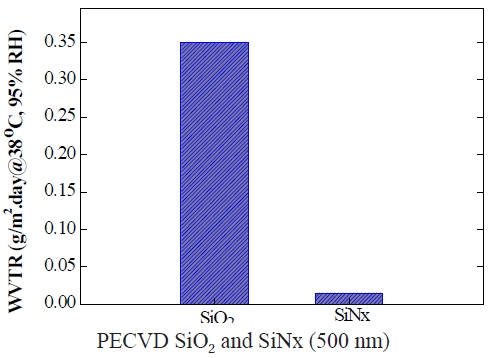
Figure 3 represents the WVTR results of SiO2 and SiNx evaporated with the same thickness of 500 nm by using the PECVD method. By applying the WVTR measurement, the values of SiNx and SiO2 were determined as 0.01 g/m2.day and 0.35 g/m2.day, respectively and SiNx showed a lower moisture penetration rate compared to SiO2 (MOCON Corp. Permatran W3/33). From the WVTR values, we found out that SiNx films have a better impermeability than SiO2 films. The benefits of SiNx over SiO2 are the lower moisture permeation coefficient and the higher electrical stability during the exposure to humidity.
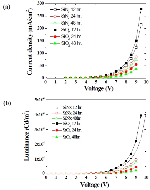
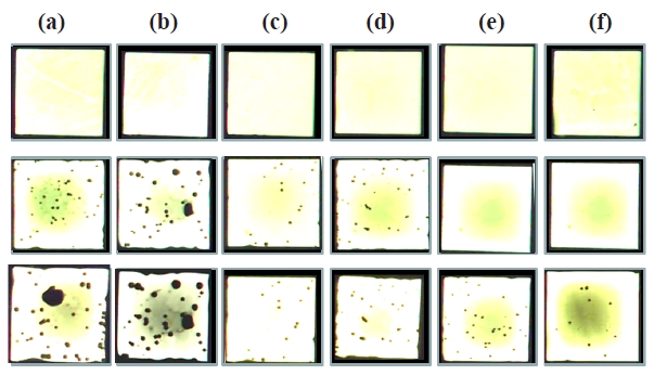
Figure 4 shows the observation results of the emitting region of the element which is evaporated by using SiO2 and SiNx with a thickness of 500 nm for creating a passivation layer on the fabricated OLED. It is stored in a constant temperature and humidity chamber with 85℃/85% for a specific period of time by using a light microscope. The observation was performed for the degradation process of the element by using a light microscope according to time (t=12 hr, t=24 hr, and t=48 hr). As shown in Figure 4 (a) and (b), in the case of the passivation layer that uses a SiO2 or SiNx single layer, it shows lots of dark spots. After 48 hours, it showed an increase in the number of dark spots and its sizes. As shown in Fig. 4 (c) and (d), in the case of the passivation layer,evaporated by using SiO2 and SiNx in shifts and it showed more excellent characteristics compared to that of a single layer only. Figure 4(e) and (f ) represent the emitting regions according to time in the structure in which multilayers of 2×{500 nm Oxide/Nitride} and 2×{500 nm Nitride/Oxide} were applied to OLED. It revealed that evaporation by using SiO2 and SiNx multilayers in shifts showed more excellent effect on the passivation layer compared to the SiO2 or SiNx single layer. Moreover, it was verified that the characteristics of the passivation layer in which SiO2 was applied as a material for the first passivation layer of the OLED showed less effect on the passivation layer than SiNx.
As the SiNx exposed to moisture shows a more stable Si-O bonding (8.26 eV) than that of the Si-N bonding (5.2 eV), it causes partial oxidation. It is easily presented in the oxide in which a strong absorption between the internal surface of pores and the surface of a passivation layer generates OH- radicals [15].
The internally generated OH- radicals exhibit correlation with the penetrated moisture. Then, it prevents the additional penetration of moisture and that leads to the decrease in the moisture penetration rate.
Regarding the evaporated SiO, Si(OH)4 can be ionized by the OH- radicals through the hydrolysis reaction as follows.
The SiNx layer showed a relatively lower value in the moisture penetration rate than the SiO2 layer at room temperature.
Figure 5 shows the characteristics of current-density and luminance-voltage in the element evaporated with a SiNx or SiO2 single layer and a thickness of about 500 nm by using the PECVD method according to time. Although the current density and luminance were decreased according to time (t=12 hr, 24 hr, and 48 hr), the OLED with the passivation by using the SiNx layer which showed a better characteristic compared to using the SiO2 layer. It was recognized that such a degradation characteristic agreed to the results of the WVTR measurement that are presented in Fig. 4 and the increase in the dark spots in an emitting region is according to time shown in Fig. 5.
In this study, an in-situ passivation method in a system was developed and the influence of the OLED on its degradation characteristics was analyzed by applying SiO2 and SiNx thin films as a passivation layer for the distribution of dark spots in an emitting region and the characteristics of J-V-L (current densityvoltage-luminance).
SiO2 and SiNx layer evaporation process with an inorganic thin film was developed by using the PECVD method. The characteristics of the thin film were also analyzed. It was possible to ensure that the moisture penetration rate in a single layer was below 1×10⁻² g/m2.day. Moreover, the fabricated OLED in which an inorganic thin film was applied to the OLEDs as a passivation layer was analyzed by applying experiments on the emitting region and the current density-voltage and luminance-voltage. Based on the results of this study, it was possible to propose the possibility of its application to flexible displays and this applies an inorganic thin film as a passivation layer. Moreover, it is also expected that the results will be used for future studies on organic-inorganic compositive passivation thin films in flexible OLEDs.