A number of surface mount technology (SMT) process variables including land design are considered for minimizing tombstone defect in flexible printed circuit assembly in high volume manufacturing. As SMT chip components have been reduced over the past years with their weights in milligrams, the torque that once helped self-centering of chips, gears to tombstone defects. In this paper, we have investigated the correlation of the assembly process variables with respect to the tombstone defect by employing statistically designed experiment. After the statistical analysis is performed, we have setup hypotheses for the root causes of tombstone defect and derived main effects and interactions of the process parameters affecting the hypothesis. Based on the designed experiments, statistical analysis was performed to investigate significant process variable for the purpose of process control in flexible printed circuit manufacturing area. Finally, we provide beneficial suggestions for find-pitch PCB design, screen printing process, chip-mounting process, and reflow process to minimize the tombstone defects.
For several decades, board level assembly techniques which employ surface mount technology (SMT) are available and most of these techniques have been developed for high-yield and costefficient microelectronic manufacturing. Due to a continuous demand for miniaturization of mobile electronics, SMT has been driven to the reduction of passive components size down. The latest generations of wireless products require more compact system-in-package (SIP) modules with nearly 01005 passives. The designation 01005 implies that the passive should be 10 by 5 mils in length and width.
In the current microelectronic package manufacturing, much complicated micro-joining technique, such as fine-pitch ball grid array (FBGA), chip scale packaging (CSP), and even through silicon via (TSV), are available or under active development [1-3]. Continuous development for newer technology may not substitute all the existing technology and moreover, for successful PCB assembly the role of SMT passives assembly cannot be neglected. It is true that fine-pitch BGA and CSP are layout with conventional SMT passives and assembly defects of SMT passives requires a good portion of the total defects per board in current board level assembly.
Different sizes of surface mount devices (SMDs) cause diverse types of defects in board level assembly, such as tombstone, component misalignment, insufficient solder, bridging, solder beading and component to component spacing. Numerous efforts have been made for several decades in the manufacturing sites of SMT development in order to minimize the assembly defects that arise from screen printing of solder paste/flux, solder mask cleaning, chip mounting, and multi-heating zone solder reflow process by even employing automatic optical inspection (AOI) at the end of assembly process. The percentage of circuit
boards that are built defect-free by the assembly process is highly dependent on the quality of the materials, design of the circuit board, and the capability of the process.
While collaborating on the development of six-sigma manufacturing strategy between academia and industry that manufactures small size display module for mobile application, we had noticed that there were increased numbers of defects-per-yield (DPY) from tombstone for a specific product manufacturing. Within a few weeks DPY were drawn to zero and this was due to the efforts of process engineers to alleviate the growing issue on increased tombstone defect but the root cause of the tombstone defect in a larger sized passives was not clearly identified.
When the chip component is raised and detached from the PCB land at one side while the remaining is bonded to the other land, it is called as Tombstone (or Manhattan) phenomenon for chip assembly. Basically during the solder paste reflow process, tombstone is caused by a difference in the solder melting time between the two lands for chip mounting. Takaki and et al., at Senju Metal Industry, had investigated the relationship between the solder alloy composition and tombstone problems, but this was investigation was carried out before the lead-free soldering was applied to the electronic products [4]. After the leadfree SMT soldering was adopted, diverse types of defects were observed such as, bridging, solder balls, mid-chip balling, poor wetting, voids, de-wetting and tombstone. Liu and Johnson reported the optimization of lead free solder 01005 component assembly in 2007 [5].
Over the years, as SMT chip components become smaller and smaller with many weighing just milligrams, the same torque that once helped in self-centering has now become a lifting-up force of components. Although the cause of the tombstone is fairly complicated, all the previous studies tend to focus on only a single process parameter as the root cause of it. The suggested process variables that contribute to tombstone defect are land design, component and board oxidation, solder paste, stencil design, screen printing, chip-mounting, and reflow.
In this paper, we have defined a number of potential process variables that contribute to tombstone defect. Moreover, we have also investigated on their correlation with respect to tombstone defect employing statistical designed experiment. Once the analysis of the experimental results is performed, we have setup hypotheses of the root causes of tombstone defect and derived main effects and interactions of the process parameters affecting each hypothesis. Finally, we provide beneficial suggestions for find-pitch PCB design, screen printing process, chipmounting process, and reflow-process to minimize the Tombstone defects.
[Table 1.] Types of SMT defects and examples.
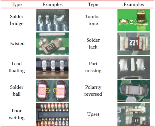
Types of SMT defects and examples.
2.1 Flexible printed circuit process
Flexible printed circuit (FPC) is a printed circuit board which is manufactured on a flexible substrate, it allows being either folded or bent to fit the available space or relative movement and commonly polyester (PET) or polyimide (PI) which has relatively low dielectric constant and good heat resistance are used. The physical advantages of flexible circuits are the primary factors that increase demand of size, shape, weight or functionality in an electronic device. The abilities of FPCs, such as reduced package size and weight, lowered assembly cost and time, and increased system reliability, had found great favor in laptops, cell phones, personal digital assistants (PDAs), and etc.
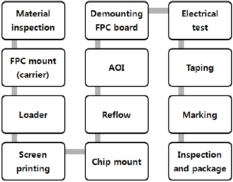
In the assembly process flow, FPC assembly seems to be quite similar to the rigid PCB assembly but the thin substrate makes the product more vulnerable to various types of defects that range from minute twist on the board to the spacing between soldering. As a result, it drags the production yield down. Typical FPC board assembly process flow is presented in Fig. 1, and various types of SMT defects are tabulated in Table 1.
As the flux and solder alloy liquefy and wet each side of the component, a small amount of torque through surface tension is applied to the component. Traditionally, the torque is applied by the surface tension of the molten solder has a self-centering capability in some extent; however, the surface tension became a serious source of assembly defect of tombstone. Tombstone is caused by minute differences in the wetting force from one side of a component to the other. When the amount of imbalance, relative to the mass of the component, exceeds certain level, the component becomes tipped upright, called either Manhattan or tombstone.
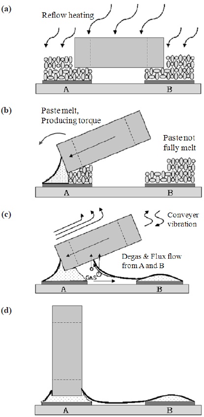
When a chip mounted board passes through the pre-heating zone of the reflow oven, in spite some amount of vibration exists in the belt furnace system, the mounted chip does not move around due to the tackiness of solder paste and flux. The board then, travels the temperature soaking and ramping up zone and this is where the tombstone defect may take place. Tombstone is caused by various system variables and process variables, and moreover in terms of processing, the direction of the board
feed through is also one of the significant factors for tombstone defect. Figure 2 depicts what may take place in the reflow oven zone in terms of the direction of the board flow. Assuming A side of land is fed first to the oven, solders on the land A may melt slightly faster compared to that of B, and increased surface tension of just the melting solder tends to produce torque to bring one corner of the mounted chip. Figure 2(b) illustrates the lifted chip by increased torque on the land A. When the lifted chip continuously passes through the elevated temperature, the rest of solder melts and the flux will flow and degas. Increased surface tension of land A continuously gathers heated flux, and eventually chips may just stand up as before cooling down. Figure 2 (b) depicts the exact process that takes place in the elevated temperature zone of the reflow oven. Some of the chips may stand up directly and some of them may be slanted.
2.3 Screening experiment for process variable selection
Over the last few decades, many researchers and SMT process engineers have taken efforts to find out the root cause of the tombstone defect, and based on the previous works done, we have initiated our research. The size of the chip components,
[Table 2.] Summary of the screening experiment.

Summary of the screening experiment.
starting from 1210 in 1980’s, continuously decreased to 0603 and 0402 in 1990’s, and currently it shrank down to 0201 and 01005. Similar to the semiconductor manufacturing industry, not only process margin continuously shrinks down in SMT assembly area, but newer issues are also being introduced in the assembly process. Although 01005 chips are used for wireless SiP (Systemin- Package) modules, most of microelectronic applications include 0603, 0402, and 0201 chips. Smaller chips are more likely self-aligned during the reflow process, but they also exhibit a tendency of tombstone defect[8]. We investigated on the influence of process variables and the interactions between process parameters on tombstone. Therefore, the size of the chip need not necessarily be small.
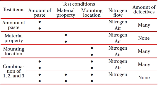
Screening experiment for effective process variable selection was performed on 1005 chip assembly by taking in to consideration soldering and mounting under five different conditions. By using Land 7 type land design, Au finished FPC and the metal mask was prepared. Four different types of lead-free cream solder pastes were applied on the FPC board, and 1005 resistor chips and 1005 capacitor chips were mounted with intentionally dislocated position of 0.1mm and 0.2 mm. On the completion of the chip mounting, reflow with/without nitrogen was followed for the prepared sample. In this screening experiment, the shape of the metal mask opening was not considered as process variables. Types of solder pastes were not a significant factor for causing SMT defects but there were certain defectives that were dependent on the size of the land. Significant amount of defects were found for the case of a different amount of solder pastes between two lands or for the case of slightly dislocated chip mounting, under the nitrogen reflow condition. Summary of this screening experiment is provided in Table 2. This result sufficiently supports the selection of the controlling factors for the SMT process control.
We have confirmed that the tombstone in FPC assembly can be affected by circuit pattern of FPC board, land design, amount of solder paste, mounting location, reflow temperature, and even the types of chip of resistor or capacitor which are in the same size. Based on the experimental results, hypotheses for the possible causes of tombstone can be established. In the FPC board design level circuit pattern and the size, shape, and gap between two adjacent lands are one group of potential causes of tombstone defect. In the screen printing sector, composition of solder paste and flux, the amount of solder paste on the lands, height and viscosity of solder paste, and shape of metal mask opening are another group of variables which cause tombstone defect. In mounting, not only the dislocation of chip mounting, but also warpage of FPC board are hidden factors for the defect. For the reflow process, with/without nitrogen application, reflow heating temperature, especially pre-heating temperature, and heat distribution on the board are significant factors for the defect.
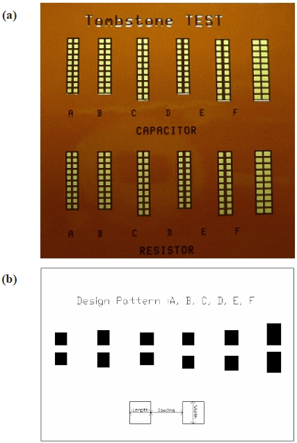
In order to ensure the established hypotheses in the previous section, we have selected 5 controllable process variables and performed experiments to find their effect on the tombstone defect as well as their relationship with each other. Chip components which we had selected were 1005 resistors and capacitors. As the shapes of the outer electrode for a resistor and a capacitor are different, the former has no metal on its sides and the latter has metal parts on its sides. Thus, the ratio of tombstone defect for capacitors is higher compared to the resistors. We also considered the direction of board feeding into the reflow oven. When the component passes the heating zone, two lands pass simultaneously and consequently passing the heating zone makes some amount of difference of applied heat to the components. Test vehicle contains two blocks for the design of experiment (DOE), and the statistical analysis was performed by using a custom built DEO data analysis tool. It includes ten lands which are designed for both resistors and capacitors, and seven different land sizes. Look for Table II for the details on experimental conditions. Design pattern and a picture of the test board are presented in Fig. 3.
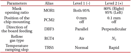
By employing the design of experiment, we have included five controllable variables, such as mask opening ratio (nominally, MOR1), position of the chip mounting (PCM2), direction of the board feeding (DBF3), reflow gas type (RGT4), and temperature ramping slope (TRS5) in pre-heat, and designed the experiment with 23 full factorial design with 2 by 2 blocks. As we have 5 variables to analyze, the full factorial design requires at least 25 runs without repetition and we were able to successively reduce the number of experiments to 23 runs with multiple blocks. The variation in the MOR and PCM was realized by metal mask design and mounting position programming. Figure 4 shows how the variables are modified in the design level for mask opening and for the mounting position, respectively. Selected parameters
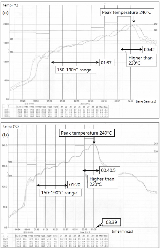
of interest and their experimental conditions in the four blocked designs are tabulated in Table 3. Moreover for further process references, two types of pre-heating zone temperature profiles, normal ramping slope and rapid ramping slope are provided in Fig. 5. In this experiment, for the purpose of experimental reference, eight test sample boards were mounted in one reflow board, and eight temperature zone reflows were used. Oxygen contents were 23% and 0.8~1% without and with
When the experimental apparatus had been setup, we performed screen printing and chip mounting in a sequential manner. In order to eliminate uncontrollable variables with time, all printing, mounting and reflow process had been performed within one day. The result of visual inspection which was performed on a dummy sample is presented in Table 4. Amount of solder varies depending on the mask opening area (MOA), and position of chip mounting (PCM) is to some extent shifted in the
[Table 3.] Selected parameters of interest and their levels.

Selected parameters of interest and their levels.
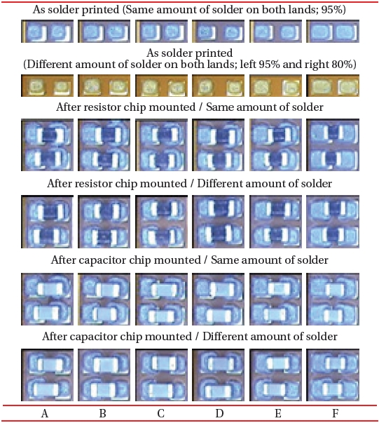
Microscopic image of the amount of solder dispensed (a comparison between same and different amounts of solder before and after chip mounting).
x-direction. In the next section, we have divided the causes of defect into three categories of pad design and process variables.
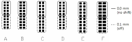
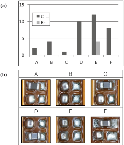
By ignoring the effects from other process variables, we have investigated the influence of land design on tombstone defects. Tombstone took place overall from sample A to F in a similar manner, some erected perpendicularly and others stood up halfway, while one side of land held the chips. Sample D, which was expanded land size and sample E, which was extended pitch between two lands showed relatively higher number of defects in the sample. In addition, C-chips presented much greater opportunity for the tombstone defect compared to the R-chips. Figure 6 presents the tombstone defects with respect to the various land designs as well as the number of defects in this experiment. This result matches well with our hypothesis of tombstone mechanism. When the land size is large the mounted chip can be dislocated to a small amount, and unbalanced wetting force on the chip causes torque to lift one side off the chip.
Considering SMT process flow, we have performed a total of eight sets of another experiment in order to look into the process
variables which can effect on the tombstone defect. This experiment was very meaningful for the process engineers to understand the complicated tombstone mechanism as it is caused by not just a single parameter, but also by the interaction between more than two parameters. As it is already suggested in Table III, experimental data has been statistically analyzed through main effect plots and interaction plots from Taguchi analysis.
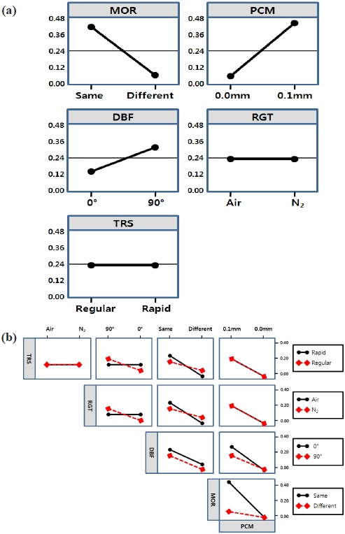
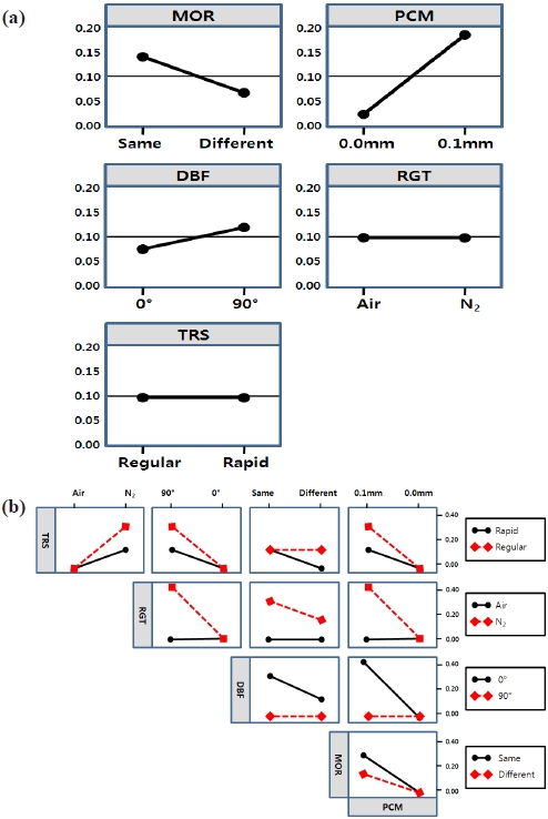
Figure 7(a) and (b) illustrate the main effect plots and interaction plots for tombstone defect on capacitor chips. Both the mask opening ratio (MOR) and the position of the chip mounting (PCM) are significant factors and moreover, the direction of the board feeding (DBF) is also significant to some extent for tombstone. Both the temperature ramping slop (TRS) and reflow gas type (RGT) were shown to be statistically insignificant. The trend of PCM and DBF are well matched with our hypothesis for tombstone, but unexpected results were observed when different amounts of solder paste via MOR. We postulated that this unexpected result came from the interaction between two or more parameters, and for further analysis the interaction plot should be investigated. It is also surprising that the temperature ramping slope (TRS) and the reflow gas type (RGT) are showed as statistically insignificant factors in the capacitor chips. Statistical interaction can be defined as the effect of one independent variable on the dependent variable which depends on the value of another independent variable. It is often confused with the term “additivity”. Additivity implies the effect of one independent variable on a dependent variable does not depend on the value of another independent variable. From the interaction plots, the two lines cross over or at least are shown not in parallel, and then the two correlated variables also have interaction to each other. In our hypothesis, unbalanced solder paste will increase the number of defects, and this was reasonable as different amounts of wetting force will be applied to the chip while it is reflowed in the oven. However in the experiment, we have not simultaneously considered it with the direction of board feeding. Thus, the analytical result may show unexpected outcomes. Nevertheless, we have successively identified the effect of chip mounting position and its interaction with the mask opening ratio.
Moreover, we also have examined the statistical significance of the parameters for resistor chips, and to some extent different results were observed. For the resistor chips, temperature
ramping slop (TRS) and reflow gas type (RGT) were observed to be statistically insignificant but other factors were significant. Similar to capacitor chips, PCM was the most significant factor and MOR also exhibited similar results to capacitors. Large amount of interaction of PCM with all the other parameters have to be carefully investigated. Figure 8 depicts the main effect plots and interaction plots of the resistor chips. From the statistical results, we have confirmed that the process variables may cause tombstone defect for resistors and capacitors are somewhat different. In a glance, two types of chips are small and identical, but the shape of the actual solder which joins is different from each other. Mechanical analysis is required for finding out the fundamentals, but it is beyond the scope of this experiment. Therefore, it is worthwhile to separate the cases of tombstone defect for resistors and capacitors.
From the hypothesis for the mechanism of tombstone defect, we have selected a set of manufacturing process variables which may affect the quality of the product. Statistical analysis based on the designed experiments was performed to investigate significant process variable for the purpose of process control in flexible printed circuit manufacturing area. In this section, we have listed some of the possible suggestions which can be utilized in the manufacturing area for the minimization of the tombstone defect. Suggestions consider land design to SMT re-
flow process.
1) FPCB design: When the tombstone takes place, SMT land design is the first factor that is to be considered. Even though the size of the components are identical, CAD designer should consider whether it is for the resistor, capacitor, or a barrister. In FPB design, for similar size of passive components, similar design rule is applied for land design but, their actual soldering contact areas are different. Designing land should be kept up with the circuit design, and it should consider design for manufacturability (DFM).
2) Screen printing: In this experiment, we have used Sn-Ag3.5- Cu0.5 and this is known for less tombstones causing solder paste. Thus, the parameter of mask opening is shown in the statistical significance. However, previous FPC assembly, misalignment of solder mask and board, the thickness of stainless steel solder mask, and the amount of solder paste printed on lands are also very important.
3) Chip mounting: The most important factor for tombstone defect that is revealed in this experiment was chip mounting. Obtaining the mounting accuracy is important, but the condition of the nozzle cannot be overemphasized. Process tools including feeder must be carefully maintained.
4) Reflow: It is the final assembly process, and various SMT defects other than tombstone that may take place through reflow process. No specific consideration other than temperature setting and reflow gas type is suggested for the improvement of the wettability of the solder. Therefore, prevention of SMT defects in design level is recommended.