Process control in semiconductor manufacturing is crucial for achieving the ultimate goals of higher product quality and reliability with lower manufacturing cost. As circuits and devices are highly integrated with the advent of 45 nm or below, tighter process control plays a very vital role to maximize manufacturing efficiency by minimizing misprocessing. Mostly plasma process control was based on the statistical methods with tool and metrology data, but advanced process control (APC) has recently emerged as a promising technique to improve the capability of process control for cost-effectiveness and higher yield [1]. By utilizing in-situ process monitoring technique, overcoming challenges in APC has become feasible and this includes real-time process fault detection.
Semiconductor manufacturing requires numerous process steps for the successful fabrication of integrated circuits (ICs), and more than 40% of the unit processes employ plasma processing in both the front-end-of-line (FEOL) and as well as in the back-end-of-line (BEOL). In the current semiconductor manufacturing, the importance of plasma processes cannot be over-emphasized while APC in the plasma process with realtime monitoring and analysis becomes increasingly important for both the current and future semiconductor manufacturing. Various in-situ sensors are used for the monitoring of plasma processes. In order to detect the electrical character of plasma, electrical devices, such as self-excited electron resonance spectroscopy (SEERS) and IV-probes have been used [2,3]. Plasma process monitoring which uses optical emission spectroscopy (OES) has also been suggested as non-invasive monitoring [4].
OES has been widely used for the monitoring of plasma process. OES measures the optical emission intensity from the glow discharge of reactive species of plasma and it provides useful information about the plasma physics and chemistry. The most well-known application of OES is end-point-detection (EPD) in etching by tracing one or more specific wavelengths and these wavelengths correspond to the etch by-products along time [5]. Moreover, it is also reported that OES can be utilized as a useful tool for in-situ real-time process fault detection and classification [6]. Despite the usefulness of OES, the selection of the corresponding wavelength peaks is arduous and this is due to representation of complicated plasma information which includes chemical species densities, electron density, and electron temperature that is in a wide range of optical spectrum. Moreover during plasma etching, it is also difficult to identify a single wavelength peak that corresponds to a specific gas due to the multiple presences of related peaks with same type of a gas molecule. For instance, we may observe more than 200 optical emission peaks that are carbon and fluorine related and they contain species from tetrafluoromethane (
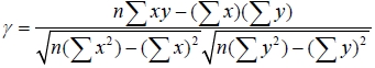
In this paper, for the analysis of OES data we present a wavelength selection method. This method uses standard deviation and correlation coefficient, and moreover, the intensities of the selected peaks are normalized by that of mostly suggested
By investigating on the data set by reactant and by-product species, separately, from the difference of abnormal etch from the baseline. Then, we found out the evidence of erosion of photoresist etch mask and this was the primary cause of the abnormal process. However, the proposed analysis was conducted offline and the suggested method can be applied for in-situ realtime monitoring of
2. WAVELENGTH SELECTION METHOD
2.1 Background of wavelength selection
Utilization of OES for plasma process monitoring requires corresponding wavelength selection. This selection is done for the analysis of chemical species and physical/chemical behaviors of gas species that are found inside the process chamber. Empirical selection of the emission spectral peaks in by-product of etch process is the most commonly used, and timely tracing of emission intensity of
2.2 Wavelength selection with engineering principle
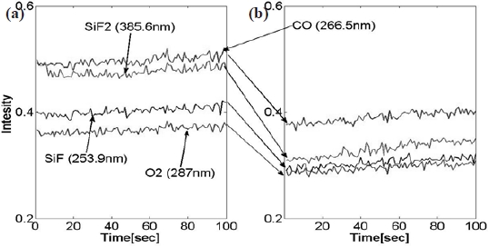
In silicon oxide etching, wavelengths may be grouped into reactant (or feeding) gases and by-products and this is done according to the mechanism of reactive ion etch. Moreover, as etching progresses the amount of ionized fluorine atoms in the chamber gradually decreases and they become saturated at some point while silicon oxide film is consistently removed. Meanwhile, the behavior of the by-product, such as
Where,
[Table 1.] Selected OES wavelengths in SiO2 etch with CF4.
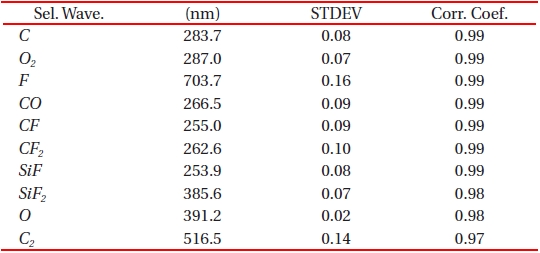
Selected OES wavelengths in SiO2 etch with CF4.
In a plasma process,
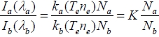
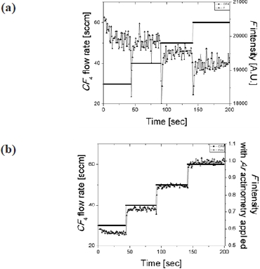
The optical emission intensity from plasma emission is the representation of photon counts at the detector, and it is true that the magnitude of intensity is a function of the distance that is found between the mounted optical fiber end and the sidewall viewport. In this research, in order to eliminate this dependency and to support engineering principle for the analysis of OES data, we employed
sidewall viewport. It is straight forward that the intensity of
Before the adoption of the chemical actinometry for the photochemical conversion of OES data set, we verified the usefulness of
3. ANALYSIS OF ABNORMAL ETCH PROCESS
In order to probe the usefulness of the emission actinometric wavelengths selection method, we have re-visited in-situ OES data which was acquired from series of experiments that were previously conducted of silicon oxide etching. ICP-RIE with 13.56 MHz RF power system was used for the etching of thermally grown silicon oxide with 50 sccm of
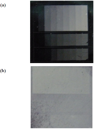
port with 10 times of integration for every 200 micro seconds. A series of etch experiments were conducted under the same etch condition and even though none of the process conditions were changed, we observed that a couple of samples were abnormally etched. Figure 3 shows two etched samples where, the one in the left is a normally etched sample and the other on the right is abnormally etched. They have line and via pattern etch in their size of 5-50 μm with AZ1512 positive photoresist mask. During the experiment no noticeable anomaly was observed and recorded. So, we applied the suggested actinometric analysis for the preselected in-situ acquired OES data. As described in the previous section, we included both the reactant and the by-product gas species along with engineering principles in plasma etch chemistry. As soon as the OES peaks for the analysis were determined,
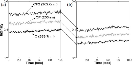
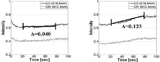
Emission actinometric analysis was performed by comparing the observed intensity of

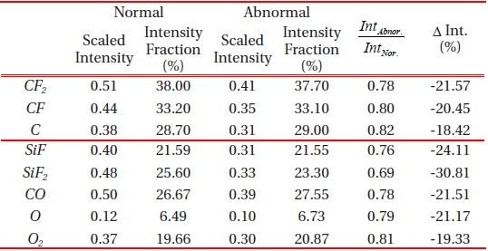
Actinometry intensity of the selected OES peaks and comparison with normal and abnormal processes.
ments of
One may simply assume that the decreased optical emission intensity is associated with the reactant gas species and can be explained with the increased emission intensity of the byproduct. On the contrary, we observed was that the emission intensity of the by-product also decreased.
the plasma to form
Optical emission spectroscopy (OES) is utilized for the analysis of abnormal etching of silicon dioxide by direct comparison with the normal process in several ways. We suggested practically simple and useful method for the selection of high dimensional OES data with significant wavelengths. By employing engineering principle before the application of previously established statistical techniques, emission peaks of reactant and the byproduct gas were separated from each other. Moreover, chemical actinometry was applied for the normalization of the radical emission intensity to and also for the elimination of the effect for the change in the electron temperate and electron density from various process gas species in the chamber. Our postulation for the lowered electron-impact dissociative ionization from this analysis as the root cause of the abnormal etch process, still remains as some extent of investigation in plasma physics. However, we report that the acquired optical emission intensities of gas species inside the etch chamber during real plasma etching are not from a confined physical experiment, is related with that of additionally created etch by-product, and they are inter-related. Utilizing optical emission spectroscopy for plasma monitoring has been useful for numerous applications, but chemical actinometry should be engaged to make emission intensity information in practical use for quantitative plasma process analysis. We remark that the chamber condition as well as RF power energy is critical in silicon oxide etching and a fragment of it which is delivered, is extremely essential in the dissociation of tetrafluoromethane (