Resistive random access memory (ReRAM) is one of the candidates for the next generation of nonvolatile memories. Various materials, such as ZrO2, NiO, and TiO2 have been proposed for ReRAM. Titanium oxide (TiO2) is attractive for ReRAM materials. TiO2 can have various valence states and electrical properties because it undergoes various phase transitions relying on thermodynamic variables, and its fabrication can be compatible with the standard complementary metal-oxide semiconductor (CMOS) process [1-6].
The scaling issue has been one of the important research topics in many emerging memory technologies. The increase of memory integration density demands the smaller structures. The most attractive structure for ReRAM is the nano-crossbar array, where the simple memory elements, have cell sizes of 4F2 per bit, when F is the half-pitch of the array [7,8]. The development of high resolution etching processes for TiO2 thin film is necessary for schemes involving nano-crossbar arrays. Until now, there have been few papers describing the dry etching of TiO2 thin film using a high density plasma source for modern microelectronic technology [9,10]. However, the dry etching method is the favored approach for the etching processes for the manufacture of integrated circuits. The most significant advantage of dry over wet etching is that it provides higher resolution potential by overcoming the problem of isotropy. Therefore, we need to understand the influence of the TiO2 etch mechanism [11].
In this study, we investigated the etching characteristics and mechanisms of TiO2 thin films using BCl3/He mixtures in an inductively coupled plasma (ICP) system. The chemical reactions on the etched surface were investigated with x-ray photoelectron spectroscopy (XPS) analysis. The elemental analysis of etched surfaces was investigated with auger electron spectroscopy (AES) analysis.
The TiO2 thin film was deposited on silicon wafer by atomic layer deposition (MP-1000, ASMGenitech: ALD), and the thick-
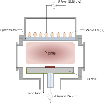
ness of the TiO2 thin film was about 100 nm. All etching experiments were performed using an ICP system. As shown in Fig. 1, the diameter of the reactor which consists of cylindrical chamber is 26 cm. A 3.5-turn copper coil located on the top of the process chamber was separated from the plasma environment by a 24 mm-thick horizontal quartz window. A 13.56 MHz RF power supply was connected to the 3.5-turn copper coil. Another 13.56 MHz asymmetric RF generator was attached to the substrate electrode for control of the DC-bias voltage. The distance between the quartz window and substrate electrode was 9 cm. The TiO2 thin film was etched in BCl3/He plasmas with variable process parameters of gas mixing ratio. At this point, the etching process conditions were performed at 400 W for RF power, -150 V for DC-bias voltage, 2 Pa for process pressure, 40℃ for substrate temperature, and the total flow rates was 20 sccm. The etched depth was measured using a depth profiler (alpha-step 500, KLA tencor). The chemical reactions on the etched surface were examined with XPS (ESCALAB 250 XPS Spectrometer, VG Scientific). The elemental analysis of etched surfaces was investigated by AES (MICROLAB 350, VG Scintific). All of the XPS and AES samples were TiO2 thin films without photoresist patterns. The etching time of the samples was 30 seconds and the sample size was 1 cm × 1 cm.
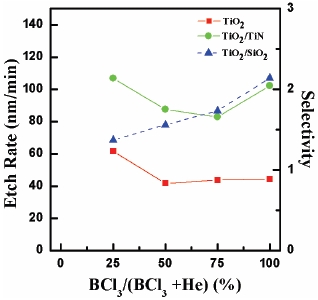
Figure 2 shows the etch rates and the selectivity results as functions of the gas ratio. The base operating conditions were 400 W for RF power, -150 V for DC-bias voltage, 2 Pa for process pressure and 40℃ for substrate temperature. As shown in the Fig. 2, the data for He (100%) flow rate is not shown because we found it very difficult to maintain stable experimental conditions in the ICP. The etch rate of the TiO2 thin film reached the maximum of 61.6 nm/min in BCl3 (25%)/He (75%) plasma. As BCl3 flow rate increased, the etch rate of the TiO2 thin film decreased. However, increasing BCl3 flow rate from 25% to 100%, the etch rate shows only small change. The selectivity of TiO2 to TiN reached the maximum of 2.13 in BCl3 (25%)/He (75%) plasma. As BCl3 flow rate increased, the selectivity of TiO2 to SiO2 increased from 1.3 to 2.13. From these results, we supposed that a physical etch pathway is more effective than chemical reaction in plasma containing BCl3. The dominance of physical etch pathway may be explained by two reasons. First, ion bombardment assisted the chemical reaction by breaking the Ti-O. Second, He gas is
related to the removal of nonvolatile compound formed on the TiO2 surface. Therefore, the grater flow rate of He compared to BCl3 means that B and Cl atoms in the BCl3/He plasma can have more opportunities to react with TiO2.
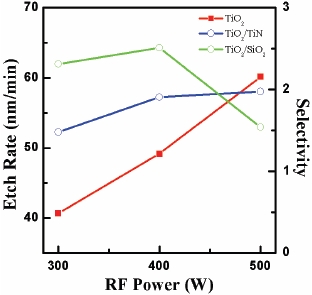
Figure 3 shows the etch rate and the selectivity of TiO2 to TiN and TiO2 to SiO2 as functions of RF power in BCl3 (25%)/He (75%) plasma. The DC-bias voltage and process pressure were -150 V, and 2 Pa, respectively. The etch rate was increased significantly as RF power increased from 300 to 500 W and reached a rate of 60.15 nm/min at 500 W of RF power. The selectivity of TiO2 to TiN showed the best value of 2.5 at 400 W of RF power. The selectivity of TiO2 to SiO2 showed the best value of 1.97 at 500 W of RF power. The increase of RF power increases the ionization and dissociation, which leads to increased ion and radical densities [12]. As the density of reactive species is increased with increasing RF power, the etch rate of the TiO2 thin film also increases. The analysis of these results indicates that the increase of RF power increases atomic Cl and He ion flow, and this leads to the increased physical sputtering and chemical reaction of Clx radicals on the TiO2 surface.
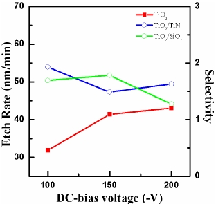
Figure 4 shows the etch rate of the TiO2 thin films and the selectivity of TiO2 to TiN and TiO2 to SiO2 as functions of DC-bias voltage. The basic process conditions of gas ratio, RF power, and process pressure were BCl3 (25%)/He (75%) plasma, 400 W, and 2 Pa, respectively. The etch rate of the TiO2 thin film increases from 31.8 to 43.1 nm/min with increasing DC-bias voltage from 100 to 200 V. The increase of DC-bias voltage can be related to the increase of ion bombarding energy, which showed as the result of increasing etch rate of the TiO2 thin film. For a high bonding strength material such as TiO2, we supposed that a strong physical component in the etching was needed to break bonds to form the etch products. Therefore, the increase of the DC-bias voltage
enhanced bond-breaking and increased sputter desorption of etch products from the TiO2 surface [12].
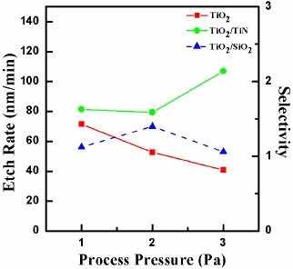
Figure 5 shows the etch rate and selectivity of TiO2 to TiN and TiO2 to SiO2 as a function of process pressure. The basic process conditions are BCl3 (25%)/He (75%) plasma, 400 W for RF power, -150 V for DC-bias voltage, and 40℃ for substrate temperature. As shown in Fig. 5, the increase of process pressure led to the decrease of etch rate of the TiO2 thin film from 71.3 to 40.8 nm/ min. Also, as the process pressure increased, the selectivity of TiO2 to TiN increased from 1.58 to 2.13. The selectivity of TiO2 to SiO2 reached the maximum of 1.39. The result of this experiment shows the following conclusions, the decrease of process pressure in BCl3 (25%)/He (75%) plasma led to the decrease of atom density and atom flux on the etched surface, but caused an increase of ion flux and mean ion energy. As a result, at the low pressure, the mean free path of the ions is longer, and this increases collisions between of particles onto the TiO2 surface, because of low energy loss due to the decreased number of collisions of the etchant species with other ions or molecules in the plasma [9].
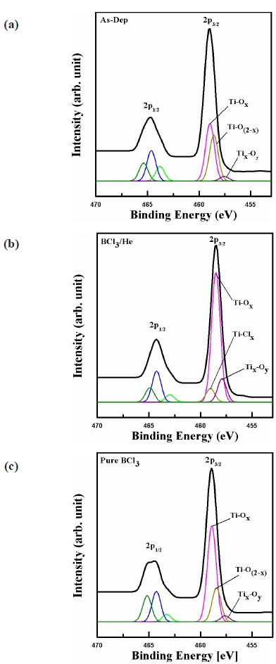
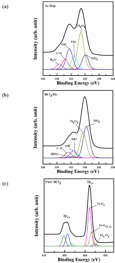
For more detailed investigations of chemical reaction, XPS analysis was performed. Figure 6 shows XPS narrow scan analysis for Ti 2p before and after etching in BCl3/He plasma. In order to analyze the chemical reaction, the etched TiO2 surfaces were compared with an as-deposited sample. Ti doublet peaks, Ti 2p1/2, and Ti 2p3/2, appeared near 464.4 eV and 458.9 eV (Δ 0.5 eV) for all the samples, respectively. Ti 2p peaks in Fig. 6 were deconvoluted to Ti-Ox, Ti-O(2-x), and TixOy peaks for the as-deposited sample, and Ti-Clx, and TixOy peaks appeard for the BCl3/He plasma etched sample [13,14]. After etching in BCl3/He plasma, the Ti 2p peaks shifted by 0.5 eV toward low binding energy. This binding energy shift was caused by changes of chemical compo-
sition of the TiO2 surface. Comparing Fig. 6(a) and Fig. 6(b), we can see the difference in chemical composition. The Ti-Clx peak appears in the Ti 2p spectra. We supposed that chemical reaction happened with the Cl-containing species and the formation Ti- Clx. As show in Fig. 6(c), the binding energy of Ti 2p is similar to Fig. 6(a). However, the intensity of Ti-Ox and Ti-O(2-x) is increased because the Ti-O bonds are destroyed by the B and Cl ion bombardments. Therefore, the chemical reactions are activated by the spontaneous surface etching [15].
Figure 7 shows XPS narrow scan analysis for O 1s before and after etching in BCl3/He plasma. The O 1s spectrum of Fig. 7 shows main peaks close to 530.5 eV. The O 1s peaks in Fig. 7 were deconvoluted to H2O, C-O, OH-, TiO, Ti2O3, and TiO2 for all samples. After etching in BCl3/He plasma, the O 1s peak shifted by 0.68 eV toward low binding energy and the intensity of Ti-O and Ti2O3 peaks are decreased. As shown in Fig. 7(c), the O 1s peak shifted by 0.1 eV toward low binding energy. The intensity of Ti-O and Ti2O3 peaks are similar to those of Fig. 7(a). As shown in Fig. 7(c), B and Cl ion bombardment produce small effects on Ti-O bonds. Therefore, the chemical reaction has not occurred as much. However, with the addition of He, the chemical reaction increases. The effect of He may be explained in two ways. First, He helps to break down the Ti-O bond. Second, He removes non-
volatile compounds formed on the TiO2 surface. Therefore, B and Cl atoms in the BCl3/He plasma can have more opportunities to react with TiO2.
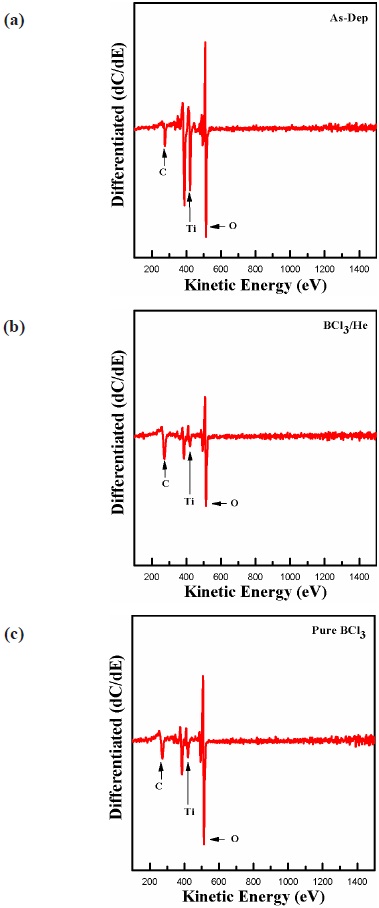
The AES analysis confirmed XPS data about the chemical reaction in the TiO2 surface. The sample size of the TiO2 thin films was 1 cm × 1 cm, and sampled were fitted into two stainlesssteel tubes of 3.5 mm internal diameter. The TiO2 thin films do not need mechanical fixing into the sleeves due to the frictional fit between the two components. The etching time was 30 sec. Figure 8 shows the composition on the surface of the TiO2 thin film obtained by AES analysis before and after etching in BCl3/ He plasma. As shown in the Fig. 8, the surfaces of all the samples were contaminated with C, O, and Ti elements. After etching in BCl3/He plasma, the amounts of O and Ti were decreased significantly. However, in pure BCl3 plasma, only the amounts of Ti element were decreased significantly, but the amounts of O element were only slightly decreased. The AES analysis explained the etching mechanism based on the physical and chemical pathways in the ion-assisted physical reaction.
In this work, we investigated the etch characteristic of the
TiO2 thin films using ICP systems. Experiments were performed with variations of BCl3/He gas mixing ratio and process pressure. We determined that the increase of BCl3 gas up to 100% led a decreased etch rate of TiO2. The maximum etch rate of TiO2 thin films was 61.6 nm/min with BCl3 (25%)/He (75%) plasma. The other process conditions were 400 W for RF power, - 150 V for DC-bias voltage, 2 Pa for the process pressure, and 40℃ for substrate temperature. It was found that the TiO2 etching depends more on physical etching and ion bombardment. From the results of the XPS analysis, we explained the chemical reaction between TiO2 thin film and B and Cl radicals. The nonvolatile byproducts that remained on the surface of the TiO2 were removed by the ion bombardments. So, the etching mechanism of TiO2 in ICP systems involved both physical sputtering and chemical reaction with ion-bombardment assistance for the best performance.