With the development of displays, such as thin-film transistor liquid crystal displays (TFT-LCDs) or electroluminescent displays (ELDs), the demand for transparent electrodes with high optical transmittance and ultra-low resistance in flat panels is increasing. The most widely employed thin films in Flat Panel Displays (FPDs) are made from Transparent Conducting Oxide (TCO) materials [1,2]. When thin films are applied to devices, their etching characteristics become important processing factors and the availability of patterning for the films is directly linked to productivity. TCO materials need to have proper etching characteristics as transparent electrodes. By far the most commonly employed TCO is Indium Tin Oxide (ITO), which is more correctly described as Sn-doped In2O3. ITO, an n-type semiconductor, offers optimum performance in terms of conductivity and transparency. In order to utilize the properties of thin films such as ITO, it is usually necessary to pattern them to create functional structures. The conventional method of patterning is the wet chemical etching process. However, this technique requires multiple process stages, large expensive machinery, and geometry patterning [3,4].
Recently, many studies on the dry etching of ITO thin films have been reported. Organic gases that contain CH4 form polymeric hydrocarbon films, which are easily deposited on etched surfaces and impede the etching process. The etching of ITO thin films using a fluorine-based gas, such as in CF4 plasma methods, has the disadvantage of inducing contamination due to polymerization. The etching of the ITO thin films by a plasma containing a mixture of Cl2 and BCl3 can lead to a fast etch rate, producing films with a smooth surface without any polymerization [5-7].
In this study, the etch properties of ITO thin films and surface reaction between ITO and the added inert gases in CI2/BCl3 plasma were investigated with an inductively coupled plasma (ICP) etch system. An analysis by x-ray photoelectron spectroscopy (XPS) was performed to understand the variations of chemical states in the ITO thin film when the surface of the film is exposed to inert gases in CI2/BCl3 plasma. Atomic force microscopy (AFM) was carried out to investigate the chemical reactions between the surfaces of the ITO thin films and etch species.
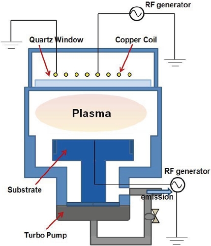
ITO thin films were deposited onto non-alkali glass using an RF magnetron sputtering system (Multi-sputtering system-b, DAEKI HI-TECH Co. Ltd.). The final thickness of the ITO thin film measured by a spectral reflectometer (ST2000-DLXn, KMAC) was about 250 nm. Etching experiments were performed to obtain the etching characteristics of ITO using a planar ICP system [8]. Figure 1 shows a schematic of the ICP etching system. The diameter of the reactor of the ICP system, which consists of a cylindrical aluminum anodized chamber, is 26 cm. A 3.5 turn copper coil was located on the top of the chamber, which was separated from the plasma environment by a 24 mm-thick horizontal quartz window. A 13.56 MHz RF power supply was connected to the 3.5-turn copper coil. Another 13.56-MHz power generator was attached to the substrate electrode to control the DC-bias voltage. The distance between the quartz window and the substrate electrode was 9 cm. The chamber was evacuated to a pressure of 133.33×10⁻⁶ Pa by using a mechanical pump and a turbo-molecular pump. The RF generators used as the core power source in the plasma apparatus provide RF power with very good stability. To generate plasma using the RF generator, a matching network unit was used to convert the loaded impedance in the plasma chamber into a 50 ohm resistance.
The etching chemistries were additive Ar, He, and N2, in Cl2/BCl3 gas mixtures with various gas mixing ratios. During the etching process, the total flow rate of the Cl2/BCl3 gas mixture was 20 sccm, and the RF power, DC-bias voltage, process pressure and substrate temperature were fixed at 600 W, -200 V, 2 Pa and 40℃, respectively. The etch rate was measured by a surface profiler (KLA Tencor, α-step 500). The analysis of the surface of the etched ITO thin films in the various etch chemistries was performed using X-ray photoemission spectroscopy (ESCALAB250, Thermo VG Scientific). The surface images of the etched ITO thin films were confirmed by using AFM (NANO Station II). The XPS studies were conducted with an MXR1 Gun-400um 15 kV spectrometer equipped with an Al Kα source. The analyzed spot size was 400 μm with the analyzer pass energy of 300.0 eV. The binding energies were referenced to the neutral adventitious C 1s peak at 284.6 eV. The AFM tip used for the non-contact mode was a silicon cantilever. The analyzed scan area was 2 μm × 2 μm.
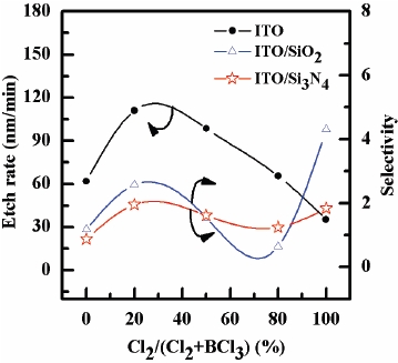
For the characterization of ITO thin films etched in an ICP system, the etch rate of ITO thin film as well as the selectivity of ITO over SiO2 and Si3N4 were investigated as functions of the gas mixing ratio. Figure 2 shows the etch rate of the ITO thin films and the selectivity of ITO over SiO2 and Si3N4 as functions of the Cl2/ BCl3 gas mixing ratio. The etch rates of the ITO thin film in pure plasmas for BCl3 and Cl2 were found to be 61.8 and 35.5 nm/ min, respectively. It can be resulted from the deposition of solid B that bonded with surface oxygen to form BxOy, as well as from the BCl radicals incorporated into the polymer-like structure[18]. The maximum etch rate of the ITO thin film was 111.1 nm/min and the selectivities of ITO over SiO2 and Si3N4 were 2.0 and 2.6 in the Cl2/BCl3 (4:16 sccm) plasma, respectively. It is well known that the chlorine components of ITO thin film form low-volatility by-products such as InClX (melting point of the InCl, InCl2 and InCl3: 211, 235, and 583℃) and SnClX (melting point of the SnCl2 and SnCl4: 247 and -33℃). We assume that the maximum etch rate is related to the effects of surface chemistry and can be explained by the chemical concurrence in ion-assisted chemical reaction. Therefore, this etching behavior indicates that at a low concentration of Cl2, the available reactive Cl radicals in the plasma assist the efficient sputter desorption of the by-products in the high fluxes of heavy BCl3 ions [9,10]. Generally, the BCl3 species enhance the etch rate of metal-oxide materials by removing oxygen in the form of species, such as BOCl, (BOCl)3, SnClX and ClXOy, or decrease the etch rate by forming non-volatile etch by-products such as InClX and B2O3. The rate of the chemical reaction in the BCl3-rich plasma is low due to the deposition of solid inorganic compounds that resulted from a complete dissociation of the BCl3 molecules. It was shown that the variation in the gas mixing ratio caused monotonic changes in the total ion density and the Cl atom density. Accordingly, we can assume the same monotonic behaviors in the fluxes of these species, and the proposed mechanism can be neglected. Therefore, the concentration of Cl2 is attributed to the BCl3 ion concentration, which tends to decrease the etch rate of ITO by forming non-volatile etch byproducts such as InClX.
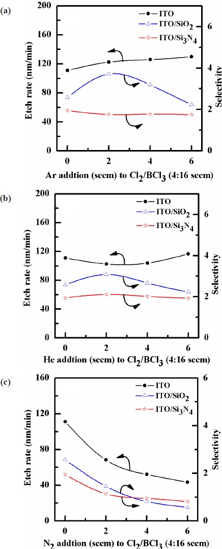
Figure 3 shows the etch rates of the ITO thin film as functions of the (a) Ar, (b) He, and (c) N2 gas contents added to Cl2/BCl3 (4:16 sccm). The flow rates of the Ar, He, and N2 added to the Cl2/BCl3 (4:16 sccm) were increased from 0 to 6 sccm. As shown in Fig. 3(a), as the Ar content in the Cl2/BCl3 plasma increased, the etch rate of the ITO thin films also increased, reaching a maximum of 130 nm/min at a gas mixing ratio of Ar/Cl2/BCl3(=6:4:16 sccm).
These findings support the assumption that, for a given range of experimental conditions, the increase of gas concentration increases the etch rate due to the physical sputtering of ions. The selectivity of the ITO to SiO2 increased from 2.58 to 3.71 as the Ar content in the Cl2/BCl3(=4:16 sccm) plasma increased from 0 to 2 sccm, and the selectivity of ITO to Si3N4 decreased from 1.95 to 1.75 as the Ar content in the Cl2/BCl3(=4:16 sccm) plasma increased from 2 to 6 sccm. As shown in Fig. 3(b), as the He content in the Cl2/BCl3 plasma increased from 0 to 2 sccm, the etch rate of the ITO thin films decreased. But, it can be seen that the etch rate of ITO thin film was 116.7 nm/min at a gas mixing ratio of He/Cl2/BCl3(=6:4:16 sccm). These findings support the assumption that, for a given range of experimental conditions, the physical sputtering of ions increases the etch rate in the case of
the increased gas concentration. The selectivity of the ITO to SiO2 and Si3N4 increased from 2.58 to 3.08 and from 1.95 to 2.11, respectively, as the He content in the Cl2/BCl3(=4:16 sccm) plasma increased from 0 to 2 sccm. But, the selectivity of ITO to SiO2 and Si3N4 decreased from 3.08 to 2.23 and from 2.11 to 1.93 as the He contents increased from 2 to 6 sccm and from 0 to 6 sccm in the Cl2/BCl3(=4:16 sccm) plasma, respectively. As shown in Fig. 3(c), as the N2 (6 sccm) content in the Cl2/BCl3 plasma increased, the etch rate of the ITO thin films decreased, and was 43.3 nm/min at a gas mixing ratio of N2/Cl2/BCl3(=6:4:16 sccm). The selectivity of the ITO to SiO2 and Si3N4 respectively decreased from 2.58 to
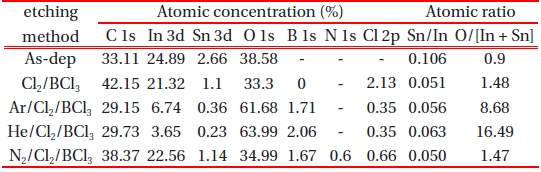
[Table 1.] Atomic concentrations and atomic ratios of ITO for various treatments.

Atomic concentrations and atomic ratios of ITO for various treatments.
0.57 and from 1.95 to 0.81 as the N2 content in the Cl2/BCl3(=4:16 sccm) plasma increased from 0 to 6 sccm. The etch rate of ITO thin film was found to be higher in the Ar /Cl2/BCl3 plasma than in the He/Cl2/BCl3 and N2/Cl2/BCl3 plasmas. The etch rate obtained by the addition of He somewhat decreased initially, but the fastest etch rate of 116.7 nm/min was observed at He content of 6 sccm. The etch rate of the ITO thin film afforded by the addition N2 decreased with increasing of N2 content in the Cl2/BCl3 plasma. The Ar and He species are ionized in the plasma and then accelerate to the surface of the ITO thin films owing to the DC-bias, which can provide energy for the reaction between the etchants and ITO thin films. For the high concentration of He, the average ion energy was lower and the chemical reaction was increased due to the increase of intensities for the Cl and B radicals. The last fact is connected with a decrease in the efficiency of ion-stimulated desorption of reaction products and can be understood from the data on ion densities and fluxes in the Cl2 and BCl3 plasmas reported in refs. [9,10]. The inert gas results in so-called ion-assisted chemical etching and, consequently, the etching rate is increased. The addition of N2 gas decreases the Cl emission intensity which leads to the decrease of the ITO etch rate [11]. These results confirm that the etch rate of the ITO films is decreased due to the lowering of the physical bombardment effect and rate of the chemical reaction.
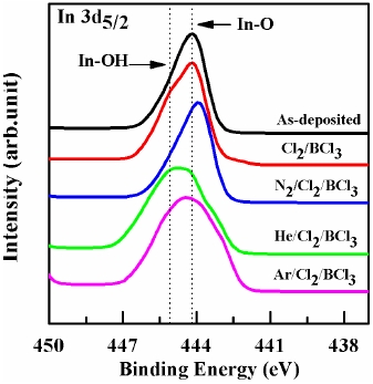
For a more detailed investigation of the chemical reaction between the ITO and etchant, XPS analysis was performed and the results are presented in Figures 4~6. The changes in the line shapes of the In 3d5/2, Sn 3d5/2 and O1s peaks were obtained as the Ar, He, and N2 gases were added to Cl2/BCl3 plasma. Table 1 shows the composition ratios obtained from the etched ITO thin film. The pronounced increase in the stoichiometric ratio of [O]/[In + Sn] and the decrease in the atomic concentration of In and C upon including Ar and He in the plasma to etch the ITO thin films provide direct evidence of oxygen enrichment near the ITO surface, resulting in the increase of the ITO etch rate. This indicates that the addition of the inert gases improved the stoichiometry of the ITO surface. As shown in Fig. 4 and Table 1, the etch reaction in the plasma with Ar occurs via the sputter etching mechanism as a result of energetic ion bombardment. In contrast, the etch reaction in the plasma including He occurs to some extent via chemical reactions forming volatile etching products [9].
shows a comparison of the In 3d5/2 core level XPS spectra with the curve-fitting results obtained from the various etched ITO samples. The In 3d5/2 peak is consistent with the presence of In3+ lattice ions [12], independent of the treatment and photoemission angle. The In2O3 and In(OH)x peaks occurred at the same binding energies of 444.0 eV and 444.8 eV peaks, respectively. The In(OH)x species probably resulted from the reaction of hydrogen with the ITO surface. The atomic concentration ratio of In listed in Table 1 dramatically decreased upon the addition of the inert gas. Table 1 shows that the decrease in the concentration of In leads to an increase in the etch rate. However, the addition of N2 gas did not lead to a change in the line shape.
This is because N2 could not supply more chlorine and did not promote the production of chloride compounds such as InClX.
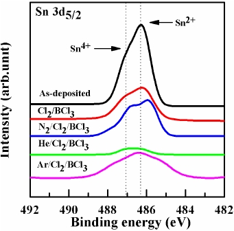
Figure 5 shows a comparison of the Sn 3d5/2 core level XPS spectra with the curve-fitting results obtained from the various ITO samples. In the case of the as-deposited ITO, the Sn2+ peak occurred at 486.2 eV and the Sn4+ peak occurred at 487.1 eV. These two peaks have been well documented due to the existence of Sn in two different oxidation states [13]. As shown in Fig. 5, the peak intensities of Sn2+ and Sn4+ on the ITO surface are dramatically decreased. This may be related to the fact that the Cl and Sn atoms have the ability to form chemical bonds with other elements. Finally, all of the treatments reduce the Sn/In ratio, indicating the selective etching of the ITO surface.
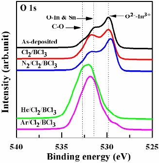
Figure 6 shows a comparison of the O 1s core level XPS spectra with the curve-fitting results obtained from the several ITO samples. The 529.8 eV peak is assigned to In2O3-like oxygen corresponding to O2- ions in the tetrahedral interstices of the facecentered- cubic In3+ lattice. The oxygen bonded to In and Sn is assigned to the 531.6 eV peak in ITO thin film. We assigned the 532.6 eV peak to oxygen resulting from C-O contamination. The O 1s binding energies of most metal oxides and hydroxides typically fall within the range of 528-532 eV. As shown in Fig. 6, the intensities of the peaks corresponding to In-O bonds were decreased by the etching process, while those of the peaks corresponding to O-In-Sn were increased. This result was attributed to the lesser reaction between the In and oxygen atoms due to the chemical reactions of the In and Sn atoms. It is considered that the plasma containing Ar and He broke the bonding of Cl with In2O3 in the tetrahedral interstices of the face-centered-cubic In3+ lattice. Therefore, the inert gas transported the reaction products such as InClX [14-16].
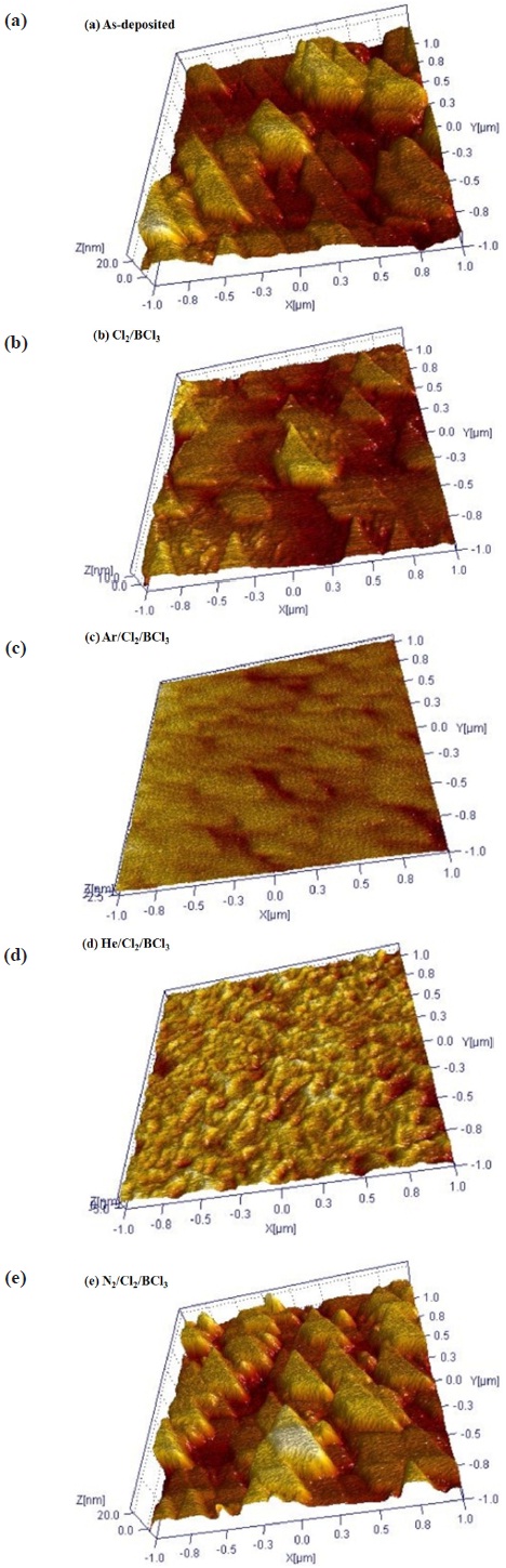
Figure 7 shows the 3D AFM images of the ITO thin film etched by the addition of different gases in the Cl2/BCl3 plasma. The RMS roughness of the as-deposited ITO thin film was 7.4 nm (Fig. 7(a)). After the etching in the Cl2/BCl3 plasma, the roughness of the ITO surface decreased to 3.4 nm (Fig. 7(b)), 0.9 nm (Fig. 7(c)), 1.7 nm (Fig. 7(d)) and 6.6 nm (Fig. 7(e)). The smoothest surface of the ITO thin film was obtained using the Ar/Cl2/BCl3 plasma, with which case the fastest etch rate was also obtained.
In this study, the surface properties of ITO thin films etched by a Cl2/BCl3 plasma containing inert gases were investigated using an inductively coupled plasma system. The investigation of the etch rate of the ITO thin film showed that the plasma including Ar produced a higher etch rate and smoother surface than those containing He or N2. The maximum etch rate of ITO thin film was 130 nm/min when Ar was added at a flow rate of 6 sccm to the Cl2/BCl3 (4:16 sccm) mixture. It is found that the reason for this maximum etch rate is the concurrence of Ar+ sputtering in the ion-assisted chemical reaction. The surface analysis by XPS showed that the binding energies of the O 1s peaks of the core levels were changed after the exposition to the exposure Cl2/BCl3 based plasma. The XPS data provides clear confirmation that the surface of the etched ITO thin film is covered by low volatility etch by-products such as InClX. The pronounced increase in the stoichiometric ratio of [O]/[In + Sn] and the decrease in the atomic concentration of In when Ar and He are included in the plasma to etch the ITO samples provide direct evidence of oxygen enrichment near the ITO surface, resulting in an increase of the ITO etch rate. The smoothest surface (RMS=0.9 nm) was obtained in the Ar/Cl2/BCl3 (6:4:16 sccm) plasma. The etching of the ITO thin films by the Cl2/BCl3 plasma containing the inert gas (Ar, He and N2) resulted in a fast etch rate and produced films with a smooth surface without any polymerization.