Recently, the fabrication of nonvolatile memory devices using room-temperature processing has attracted substantial attention, since plastic-based devices, as one of the promising nextgeneration devices, are vulnerable to heat [1-7]. Among the various nonvolatile memory devices, a nano-floating gate memory (NFGM) structure containing nanoparticles (NPs) embedded in gate layers has been considered as a strong candidate for nextgeneration nonvolatile memory devices, owing to the reliability of its charge retention and endurance [8-10]. In particular, metal NPs with a high work-function have been actively utilized for high performance NFGM devices, since they play a role in efficient charge storage with good retention properties [11-13]. Up to now, NFGM devices composed of metal NPs with a high workfunction have been made by solution-processable fabrication at room temperature [14]. Nevertheless, solution-processable fabrication has difficulties in terms of its reproducibility and imposes limits on the fabrication of 3-dimensioinal structures such as nanowire-based TFTs or FinFETs. Therefore, in this study, we propose a new procedure for the room temperature fabrication of NFGM devices utilizing platinum (Pt) NPs prepared in a sputtering system with a cooling unit. Pt with a work-function of 5.65 eV is a representative metal with a relatively high work-function.
Silicon (p-type, (1 0 0) orientation) wafers with 6.3-nm-thick thermally grown oxide layers were utilized as the substrates. Pt NPs were formed on the SiO2 layers used as the tunneling oxides by the DC magnetron sputtering method. A Pt target was sputtered for 10 s under Ar gas at a pressure of 3.0 mTorr with a sputtering power of 25 W. Then, control oxide layers of SiO2 with a thickness of 45 nm were deposited by the RF magnetron sputtering method under an Ar and O2 atmosphere. During all of the sputtering processes, the temperature of the substrates was maintained at 290 K with a water-cooling unit. Finally, top electrodes of Au were deposited on the control oxide layers by the thermal evaporation method. The structure and electrical characteristics of the devices were examined by high-resolution transmission electron microscopy (HR-TEM; Tecnai G2 F30) and a semiconductor parameter analyzer (HP 4285A), respectively.
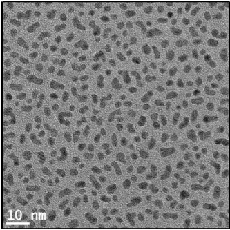
The HR-TEM image of the Pt NPs sputtered at room temperature is shown in Fig. 1, revealing a discrete morphology with an
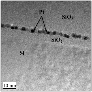
average size of 4 nm. The density of the Pt NPs estimated from the HR-TEM image is about 3.2×1012 cm-2. The cross-sectional HR-TEM image shown in Fig. 2 clearly indicates that the Pt NPs are formed separately from each other and situated between the tunnel and control oxide layers.
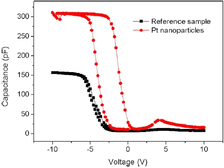
The high-frequency capacitance-voltage (C-V) curves taken at a frequency of 1 MHz with a sweep rate of 0.2 V/s are plotted in Fig. 3. While the C-V curve of the MOS capacitor without any Pt NPs shows a negligible flat-band voltage shift when the gate voltage is swept from 10 V to -10 V, the C-V curve obtained for the Pt NP-embedded MOS capacitor has a flat-band voltage shift of about 3.3 V in a counterclockwise direction. The significant flat-band voltage shift is due to the presence of the Pt NPs. The observation reveals that charge trapping in the Pt NPs embedded in our MOS capacitor occurs through the injection of electrons from the p-Si substrates into the Pt NPs. The amount of charge carriers stored in the Pt NPs can be estimated by the following relation:
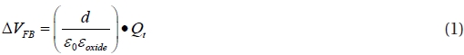
where ΔVFB is the value of the flat-band voltage shift (3.3 V), d is the tunneling oxide thickness (6.3 nm),
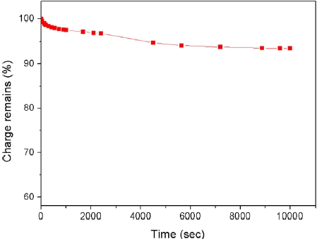
The charge retention characteristics of the Pt NP-embedded
MOS capacitor were examined through capacitance versus time (C-t) measurements. The Pt NP-embedded MOS capacitor was charged for 1 s at a bias voltage of -10 V, and the C-t measurement was then performed under a stress voltage of -5 V.
The remaining charge is defined as follows:
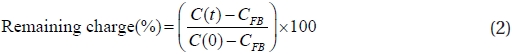
where C(t) and C(0) are the capacitance at the measurement time and the initial capacitance, respectively. CFB is the flat-band capacitance during the forward bias sweeping. Figure 4 shows the excellent retention characteristics of our device, indicating that more than 93% of the charge remains even after 104 s.
In this study, we fabricated Pt NP-embedded MOS capacitors using a sputtering system at room temperature. Pt NPs with a density of 3.2×1012 cm-2 were formed separately from each other and situated between the tunnel and control oxide layers. The amount of the electrons stored in each of the Pt NPs was estimated to be 0.7 for the flat-band voltage shift of ~3.3 V when the gate voltage was swept from 10 to -10 V. In addition, 93% of the charge remained even after 104 s, indicating good retention characteristics of the Pt NP-embedded MOS capacitor.