A biosensor can be defined as a device that detects biomolecules and is able to convert the measurement to electrical signals [1-3]. Most biosensors consist of transducers and receptors. The receptors detect the target molecules, while the transducers convert the collected signals. Response of a biosensor to a target molecule is usually in proportion to its concentration. The signal is then sent to an analyzing system. The biosensors are specialized for detecting biomolecules by introducing antibodies, proteins or enzymes on the transducers. The characteristics of the transducer are critical to determining the performance of the biosensors.
One-dimensional FETs exhibit noticeable current modulation, when the ambient is changed compared to planar structure devices, due to their large surface-to-conducting channel volume. Additionally, 1-D FETs show stable and consistent electrical performance, because a 1-D structure channel is expected to have further improved electrostatic gate control, compared to a 2-D channel [4]. Therefore, 1-D nanomaterials are an excellent candidate channel material in field-effect transistors (FETs), for the direct detection of biomolecules. For device fabrication, 1-D FET type biosensors have been fabricated with a bottom-up approach. Silicon nanowires have been widely used for biosensors [5,6], while other 1D structures have also been extensively investigated. Carbon nanotubes [7,8] and metal oxide nanowires [9-12] have been employed for biological detection. Recently, conducting polymers [13] have also attracted attention, due to their advantages of fabrication process and cost.
When nanomaterial sensors were initially investigated, pristine nanostructure FETs were used for chemical and bio-sensors, without any functionalization of the channel surface [14]. H+ ions, as well as Na+, K+, Ca2+, and Mg2+ ions, have been detected with n-channel MOS transistors. Pristine nanowire FETs have also been employed as gas sensors, and biosensors for detecting hydrogen and penicillin, respectively [15]. However, since the pristine channel surface of the FET can react with various kinds of molecules, it is difficult to extract the signal of one specific type of target molecules. In order to distinguish the mixture of components, Chen et al. demonstrated a hybrid gas sensor, composed of In2O3, ZnO, SnO2 nanowires and SWNT (single-walled carbon nanotubes). They used a statistical method called princi-
pal component analysis (PCA), for analyzing conductance. NO2, H2 gas and ethanol have been examined, and NO2 gas can be distinguished, but there is a slight overlap between ethanol and hydrogen clusters [16]. However, the fabrication of the hybrid array is complicated, and gas discrimination by the statistical method is only useful for certain mixtures. Direct modification of channel surface enables the biosensor to distinguish specific target molecules. When the surfaces of conducting channels are modified with receptors that react with matched target molecules, the FET based sensors show conductance modulation only to the presence of the target molecules. For example, specific binding between the Biotin-Streptavidin pair has been introduced to silicon nanowires (SiNW) biosensors, and biotin-modified SiNWs show good selectivity to Streptavidin [17,18].
In the following sections, we review a couple of key process steps, alignment and functionalization of nanostructures to realize biosensors. The functionalization section is broken down into two parts: devices that use a gate dielectric, and devices that use direct functionalization. Additionally, we review detection and conduction mechanisms of the devices [19-26].
2. ALIGNMENT OF 1-D NANOMATERIALS FOR BIOSENSORS
Among various integration processes to fabricate 1-D FETs, it is critical to place nanomaterials at desired locations simultaneously. One of the most common methods to locate the nanomaterials into a designed place is based on luck, through randomly spreading nanomaterials on a patterned wafer. Unfortunately, this process is difficult, and slow to build and identify a working device. A novel technique is needed in order to produce devices in large quantities. Various methods have been proposed, such as electrically and chemically assembled processes, to achieve a facile way for wafer scale integration of 1-D nanomaterial devices.
When an electric field is applied to a nanomaterial in liquid suspension, it polarizes the nanomaterial, forcing it to align, with its length oriented parallel to the direction of the electric field. The alignment quality is dependent on many factors, including the field strength and thermal energy. Additionally, the length of the nanostructures has also been found to be a factor, because of the alignment strength’s dependence on the anisotropy in electric polarization. When a small number of SWNTs are aligned, a DC electric field resulted in effective alignment. On the other hand, it is found that an AC electric field proved to be useful in arranging a high density of SWNT [27]. By applying a DC electric
field on two gold substrate electrodes, localized growth of SiNW, without an additional alignment step, has been also introduced [28].
Another technique for alignment of nanomaterials uses electrostatic coulombic interactions with substrate surfaces. For example, since SiO2 substrates usually show negative charges, it is necessary to modify a surface charge of the nanomaterial into a positive charge, to assemble them on the patterned substrate area. In the case of silicon nanowires, SiNWs have been modified with 3-amino-propyl-triethoxysilane (APTES) to have a positive charge at pH 7. It is noted that the functional group polarity of the modified surface is determined by the pH of the solution. The amine functional group becomes positively charged (-NH3 +) at pH 2 [29,30]. while the carboxylic acid functional group show positive, even above pH 7 [31]. In particular, once the metal oxide surfaces are functionalized by APTES, the nanomaterials do not require additional treatment for the amino acid functionalization process.
Contact lithography has been introduced to prepare highly dense SiNW arrays, using poly(dimethylsiloxane) (PDMS) and water soluble glue. In this method, SiNWs have been transferred from an original substrate to a target place [32]. Focused ion beam (FIB) deposition has been also suggested, to provide a direct metal interconnection between a 1-D nano-material and a source/drain electrode [9,33]. Since the deposition can be targeted on the nanomaterials directly, it is appropriate to fabricate a single nanotube/nanowire device.
3. FUNCTIONALIZATION OF NANOMATERIALS
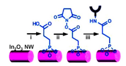
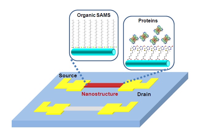
As mentioned early, surface modification of a transducer is a critical step in preparing highly sensitive and selective biosensors. Nanomaterials have been frequently modified with biomolecules and chemicals, by immersing them into solution. Depending on the type of nanomaterial that is used for a conducting channel, a different strategy for surface functionalization can be selected. Due to their high reactivity, metal oxides such as TiO2, ZnO and SnO2, as well as SiO2, are good candidates for surface functionalization. Various types of self-assembled monolayers (SAMs) have been introduced for modifying the oxide surface. Since the SiNWs have a native oxide layer on the surface, the surface functionalization of SiNWs is compatible with metal oxide nanomaterial functionalization. Therefore, similar chemistry has been announced in both SiNWs and metal oxide nanowires (and nanotubes). For example, carbonyl groups [34] provide a covalent bond to the oxide surface. The silanol group and the phosphoric acid group also have high affinity to create covalent bond to the oxide surface (Fig. 2)[35-37]. Certainly, properties of the modified surface depend on the functional group of SAM layers, such as selectivity to H+ ions with amine terminated SAMs.
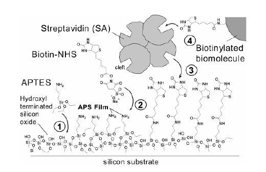
Now, let us discuss functionalization of individual nanomaterials, and their applications. SiNWs are extensively investigated, because of their compatibility with Si-based microelectronics. Various sensor applications have been demonstrated [6,38]. Initial SiNW based biosensors are reported by the Lieber group in 2001. The SiNW based FETs successfully detect bio-substances in aqueous solution by functionalizing the surface with receptors such as amine terminated silanol, biotin and antigens [18]. For instance, biotin-modified SiNWs show a high sensitivity to the existence of streptavidin in the pico-molar range [39]. Figure 3 shows the SiNW based biosensors that are modified by biotin to provide selective binding with streptavidin [40]. In another example, they use bio-functionalization to attach antibodies specific to Influenza A, allowing the virus to be detected by an individual nanowire device [41].
Metal oxide nanomaterials have been also studied with various surface functionalization methods. The functionalization with proteins on the metal oxides has been demonstrated using covalent bonds between the metal oxide and the branch of the protein that consists of amine (-NH3) and carboxylic acid (-COOH). For more stable binding, nanomaterials need to be modified with a specific SAM layer that has higher affinity to proteins than oxide surfaces. For example, the nanowires are immersed into 3-(trimethoxysilyl) propyl aldehyde solution, and the antibody is activated using the amine functional group [42]. Then the aldehyde layer present in the nanowire reacts with the amine-terminated antibodies, due to a very strong covalent chemisorption. For immobilizing proteins or antibodies, functional organosilanes, such as (3-glycidyloxypropyl) trimethoxysilane (GPS), (3-mercaptopropyl) trimethoxysilane (MTS)[43], are also applied on the metal oxide surface. Due to the presence of a functional group in the organosilanes layers, proteins or antibodies can be settled down on the functionalized surface. For detecting combinations of DNA, Curreli et al. have employed In2O3 nanowires [12]. By treating the nanowire with a phosphoric acid solution, single-stranded DNA can be immobilized on the nanowires. The DNA-functionalized nanowires enable to detect another single-strand DNA or single stranded DNA binding protein [44].
Since the introduction of semiconducting carbon nanotube FETs in 1998, SWNT FETs have been successfully transformed into biosensors with surface functionalization [45]. By replacing the solid-state gate with detecting molecules, the nanotube conductance can be modulated by target molecules [8]. However, in contrast with the metal oxide surface, the SWNTs have a chemically stable surface that it is difficult to be functionalized. Two methodologies have been introduced for surface functionalization of the SWNTs. One is indirect functionalization, where the nanotube is coated with polymers that have many functional groups. For example, SWNTs were coated with a mixture of two conducting polymers (CPs): polyethyleneimine (PEI)[46] and
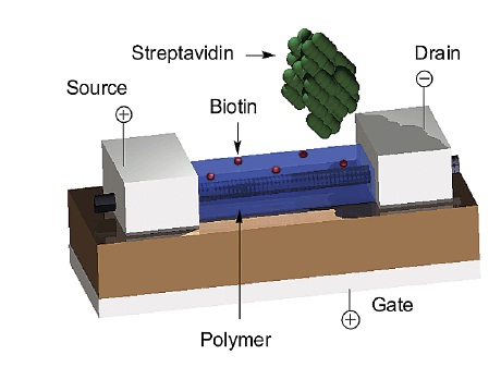
polyethyleneglycol (PEG) [17]. The PEI provided amino groups for further coupling to biotin-N-hydroxy-succinimidyl ester [8]; the PEG prevented nonspecific adsorption of proteins on the functionalized carbon nanotube. The control experiments revealed specific binding of the streptavidin, which occurs only on the biotinylated interface. By biotin modification with polymer coating, the SWNT FET can be successfully altered to its function as a biosensor that is sensitive to streptavidin (Fig. 4)[17]. The second technique is direct functionalization, where the nanotubes are modified with receptor molecules. Because of the inert nature of SWNTs, it is difficult to modify the nanotube wall. The receptor molecules can be fixed only on the edges of the nanotube with covalent bonds [47].
Since conducting polymers have been frequently used to modify the SWNT surface, attempts have been made to integrate the conducting polymers themselves as the channel materials. The advantage of the conducting polymer nanowires is their ability to be directly functionalized, much like metal oxide nanomaterials. Biomolecules can be also incorporated into the conducting polymer in a single step during polymer synthesis, rather than the multiple steps which are required for synthesis of surface-modified silicon nanowires and carbon nanotubes [48]. Field-effect transistors based on CP single nanowires, such as polyaniline, polypyrrole and poly(3,4-ethylenedioxythiophene), were fabricated and characterized [19].
4. MECHANISM OF ELECTRICAL DETECTION
Absorbed biomolecules on 1-D semiconducting nanomaterials frequently affect their electrical conductance. When the surface of the nanomaterial is modified with bio-receptors, the electric field due to the charged biomolecules on the surface causes depletion or accumulation of charge carriers in the 1-D materials. The electric field perpendicular to the surface shows the function of a biomolecule concentration. The device structure is analogous to FETs.
The facile electron transfer between Cytochrome C (cytc), which is a well characterized as an electron transport protein, and the SWNT indicates that the adsorbed protein acts as a redox center. The modulation of electrical conductance of the SWNT results from an electrostatic gating by Cytochrome C [49]. A similar model is also applied to the conducting polymer (CP) nanowires based biosensors for glucose detection [50]. CP nanowires are coated with a redox enzyme called glucose oxidase (GOx). GOx is reduced after oxidizing glucose. The negatively charged GOx modulates conductance of the CP nanowires. With this sensing method, FET type glucose biosensors using SWNTs and metal oxide structures have been also developed [11,51].
When charged molecules exist on the surface of the FET
biosensors, the channel can be controlled by the electric field generated by the adsorption of charged biomolecules. This is equivalent to applying a gate voltage. The threshold voltage (VT) and the drain current (IDS) of the MOSFET-type biosensor can be defined as follows [52]:


where ΦMS is the difference of work function, Φf is the Fermi potential of the semiconductor bulk, Q0 and Qd are the charge per unit area at the interface and bulk of oxide, and in the depletion region, respectively. C0 is the gate oxide capacitance per unit area, μ is the surface mobility of minority carriers in the semiconductor, and W and L are the width and length of the gate, respectively. Finally, VGS is the gate to source voltage, and VDS is the drain to source voltage.
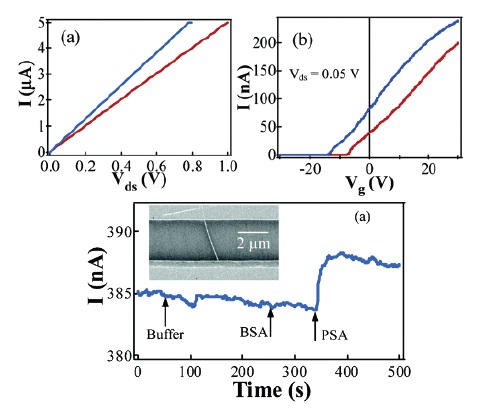
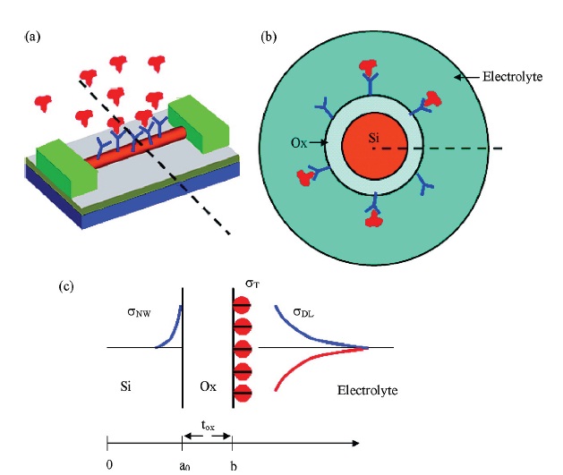
Based on the FET model, electrical properties of In2O3 nanowire FETs have been investigated. The In2O3 nanowire FETs have been treated with a prostate-specific antigen (PSA) solution [53]. The characterizations of current-voltage (I-VDS) and current-gate voltage (I-VG) characteristics were performed before and after the treatment. After the treatment, conductance of the nanowires devices increases, as shown in Fig. 5. Conductance versus time was plotted, and indicated a charge-transfer interaction between the antibodies and the virus [41]. However, in the presence of a buffered solution, the charged biomolecules are not effective in modulating the current, because of the electrostatic screening by ions in the electrolyte. Alam group suggested a screening-limited response model with SiNWs [25]. Starting from a simple capacitor model, the conductance modulation of SiNW biosensors can be derived. The value of the charge density due to analyte molecules (σT) is equivalent to the sum of the net charge in the electrical double layer (σDL), and the charge induced in the sensor (σNW). σDL represents the screening due to the ions in the electrolyte (Fig. 6).
Another phenomenon which affects conductance in biosensor FETs is carrier mobility reduction, due to an increase in the number of charge scattering sites from adsorbed biomolecules [54]. A randomly distributed scattering potential generated by the absorbed biomolecules modulates the mobility (μ) of the charger carrier. A reduction in mobility causes a corresponding decrease in the current level. However, the carrier concentration and the mobility changes cannot be separately characterized by conductance measurement, since conductivity is defined as σ=neμ. Transistor measurements of the transfer characteristics, however, can distinguish between these two mechanisms [55].
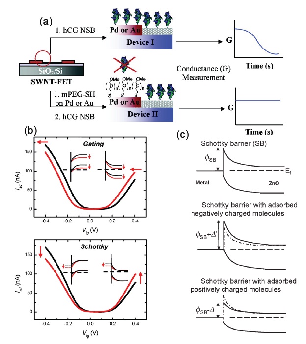
Some researchers have developed theories of conductance changes involving contact barriers between the channel and the electrode. Associated analyte molecules are polarized. As a consequence, induced dipole moments shift the work function of the metal electrodes in contact with the semiconducting channel. H. Dai’s group suggested the Schottky barrier mechanism, by passivating source and drain electrodes in the SWNT FET biosensors [56]. After blocking the contact areas, to avoid exposure to biomolecules, the amount of conductance modulation has been decreased. Based on this result, H. Dai et al. claimed that the main reason for conductance changes is due to Schottky barrier height modulation [56]. Research by the Dekker group also demonstrates that the adsorbed biomolecules at the metal contact modulate the local work function, and thus the band alignment. Even though the Dekker group employ the Schottky barrier mechanism, they concluded that the combination of electrostatic gating and Schottky barrier effects is the major contribution for conduction modulation [57]. In metal oxide based biosensors, Wang et al. also suggested the Schottky barrier model for ZnO nanowire based FET biosensors [9]. The response to the charged biomolecules is explained by using a band diagram of a metal and ZnO nanowire contact (Fig. 7). When the charged molecules are adsorbed near the junction region, Schottky barrier height and width are modulated, which results in a conductance drop. However, for most SiNW biosensor applications, the heterogeneous contact issue can be eliminated, by passivating the contact area.
5. FUTURE PERSPECTIVES AND CHALLENGES
The alignment, surface functionalization and detection mechanism of nanostructure based FET biosensors have been reviewed in this article. Recent results show that 1-D nanostructure based FET biosensors are promising for applying to future biosensor technology. However, the practical manufacturability of biosensors is still an issue to be overcome. Because of the high cost and complexity of the fabrication steps, mass production has not yet been realized. For practical biosensor applications, the biosensors should be highly reproducible, which brings accurate analysis.
Although several conduction models described in this paper suggest detection mechanisms in the biosensors, they still suffer from a huge variation in verifying the model. Unreliable electrical contact also affects the variation of biosensor properties. Even though there are some obstacles to be overcome, recent dramatic progress in 1-D nanomaterial FETs will lead to practical nano-scale biosensor applications in the near future.

![Surface modification of In2O3 nanowires with phosphoric acid terminated SAMs. Antibodies have been substituted for detecting antigens [53].](http://oak.go.kr/repository/journal/11399/E1TEAO_2012_v13n4_165_f002.jpg)
![Scheme of biotin modification of SiNW for detecting streptavidin [40].](http://oak.go.kr/repository/journal/11399/E1TEAO_2012_v13n4_165_f003.jpg)
![SWNT based FET biosensors for detection of streptavidin with poly(ethylene glycol) (PEG) coating [17].](http://oak.go.kr/repository/journal/11399/E1TEAO_2012_v13n4_165_f004.jpg)
![I-VDS and I-VG shifts of an In2O3 nanowire device before (Red) and after (Blue) PSA incubation. The bottom graph shows current variation of real-time measurement of the In2O3 NW device [53].](http://oak.go.kr/repository/journal/11399/E1TEAO_2012_v13n4_165_f005.jpg)
![(a) SiNW is functionalized for biosensor applications, (b) crosssectional view of (a), (c) diagram of charge distribution in the SiNW based biosensor [25].](http://oak.go.kr/repository/journal/11399/E1TEAO_2012_v13n4_165_f006.jpg)
![(a) Schematic of surface functionalization of SWNTs with Human chorionic gonadotropin (hCG) before and after modification of S/D electrodes [56], (b) electrostatic gating effect on Schottky barrier of SWNT FET [57], (c) explanation of the response of the ZnO Schottky- gated device to the charged molecules [9].](http://oak.go.kr/repository/journal/11399/E1TEAO_2012_v13n4_165_f007.jpg)