The rapidly increasing use of transparent and conductive oxide (TCO) films for large-area displays and solar cells has prompted the development and study of inexpensive TCO materials, which exhibit appropriate optical and electrical properties.
Recently, Al and Ga doped ZnO films have attracted attention due to their high optical transmittance in the visible wavelength range, low electrical resistivity, and relatively low cost compared to Sn-doped indium oxide (ITO) [1,2] films.
However, in most metal doped ZnO films, relatively high substrate temperatures are required in order to obtain the necessary electrical conductivity and optical transmittance in the visible wavelength region [3,4]. Thus, for certain applications, such as flexible optoelectronic devices, high substrate temperatures are undesirable due to the low thermal resistivity for polymer substrates [5,6]. One way to improve the optical and electrical properties of the TCO films without substrate heating is to use TCO/metal/TCO structures that have lower resistivity compared to TCO single layer films of the same thickness [7-9].
In this study, transparent and conducting GZO/Cu bi-layered films were deposited on a glass substrate without intentional substrate heating by RF and DC magnetron sputtering and then the effect of the Cu bottom layer on the optical, electrical and structural properties of the films were investigated.
GZO/Cu bi-layered films were deposited on a glass (Corning 1737) substrate without intentional substrate heating by RF and DC magnetron sputtering equipped with two cathodes. RF (13.56 MHz) and DC power were applied to the GZO (purity; 99.99%) and Cu (purity; 99.9%) targets, respectively. During deposition, the substrate temperature was monitored using a K-type thermocouple in direct contact with the substrate surface and was maintained at 60℃.
Prior to deposition, the chamber was evacuated to a pressure of 2.0×10⁻⁴ Pa. Sputtering was performed at 1×10⁻¹ Pa in argon (Ar) and the deposition distance between the target and substrate was maintained at 7 cm. By controlling the deposition time and
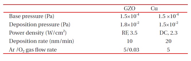
[Table 1.] Deposition conditions of GZO and Cu thin films.

Deposition conditions of GZO and Cu thin films.
sputtering power, the thickness for GZO film was maintained at 100 nm, while the thickness for the Cu bottom layer was set at 3 and 5 nm, respectively. For comparison, 100 nm thick GZO single layer films were also deposited under the same deposition conditions. Table 1 shows the deposition parameters and conditions in this study.
After deposition, film thickness was confirmed with a surface profilometer, and the crystallization of the films was observed with high resolution X-ray diffraction (XRD, X’ pert Pro MRD, Philips at Korea Basic Science Institute, Daegu Center). The root mean square (RMS) roughness was analyzed using atomic force microscopy (AFM, XE-100, Park Systems). In addition, optical and electrical properties were assessed using a four-point probe (Loresta-EP, MCP-T360, Mitsubishi) and a UV-Vis. spectrophotometer (Cary 100 Cone, Varian), respectively. The glass substrates showed a 92% optical transmittance in the visible wavelength range. The performance of the GZO and GZO/Cu films as transparent conducting films was evaluated using the figure of merit (FOM) [10].
In order to evaluate the performance of the GZO/Cu films, structural characterization is very important since the optical and electrical properties of the films are strongly dependent on the microstructure. Recently, Sun et al. investigated the initial growth mode of ITO on glass substrate over a substrate temperature range of 20-400℃ [11]. They suggested that an amorphous structure ITO film was formed at substrate temperatures below 150℃.
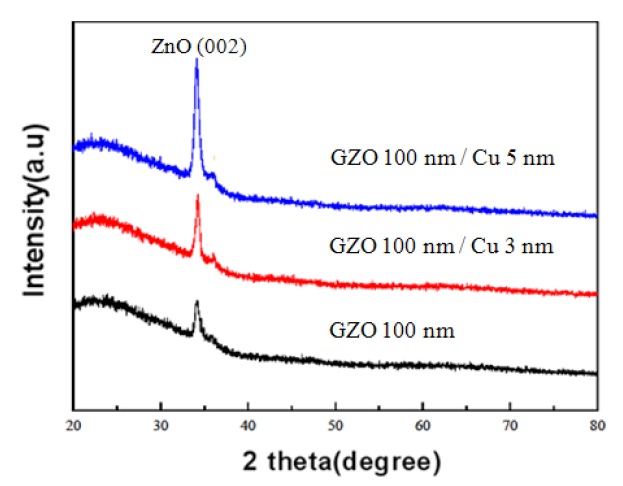
Figure 1 is the XRD patterns of GZO and GZO/Cu bi-layer films deposited without intentional substrate heating. For all of the films, the diffraction peaks in the XRD pattern were identified as (002) plane of a ZnO film.
Although the Cu bottom layer did not show any diffraction peak in the pattern, it is observed that as the Cu thickness in-
creased, the peak intensity of ZnO (002) increased proportionally.
Thus, it is supposed that the Cu bottom layer may enhance the crystallization of the upper GZO films. In a previous study, Y. Kim reported similar results that in ITO/Au bi-layered films, the crystallization of the ITO film is promoted by the Au bottom layer [12].
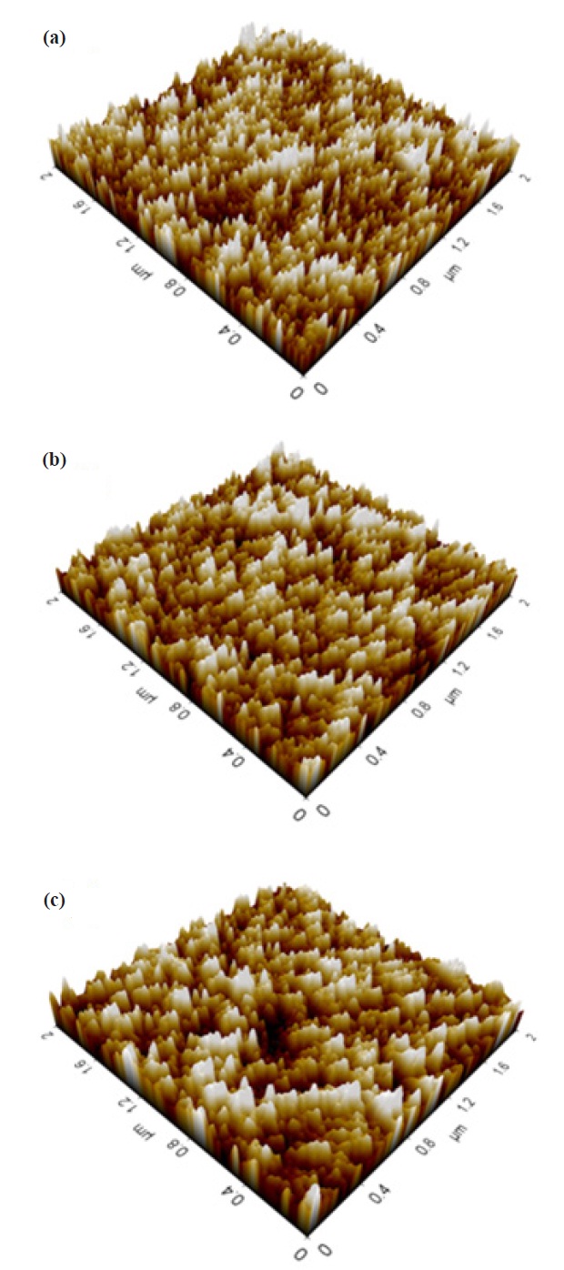
Figure 2 shows the three-dimensional AFM images of asdeposited Cu and GZO/Cu films. The RMS roughness of the asdeposited 3 nm thick Cu thin film was 0.30 nm and 0.52 nm for 5 nm thick Cu thin film was 0.52 nm, respectively. With increasing the thickness of the Cu bottom layer, the RMS roughness of GZO/ Cu films was increased. The higher RMS roughness of 3.9 nm was obtained from the GZO 100 nm / Cu 5 nm bi-layered films.
As shown in Fig. 2, though the thin Cu bottom layer had a relatively flat surface morphology, it increased the surface roughness of the GZO film effectively in the bi-layered films. Since the rough surface morphology resulted in a wider film surface area, it can be inferred that the effect of the Cu bottom layer on the surface roughness is favorable for solar cells and gas sensor applications regarding GZO films.
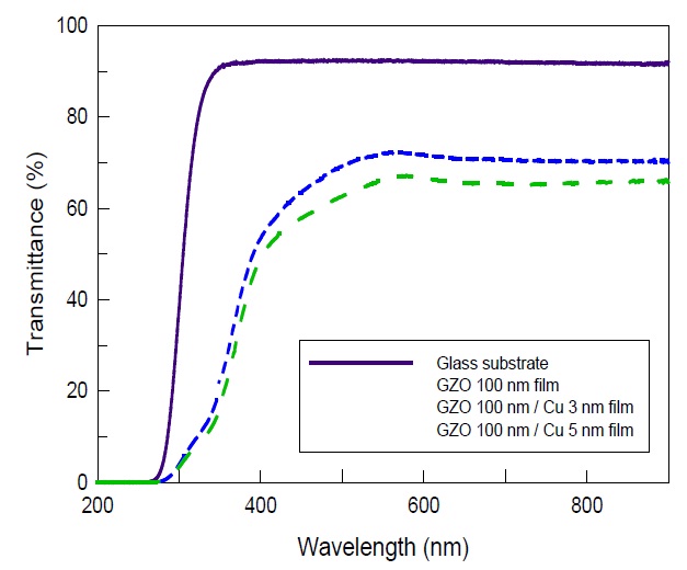
Figure 3 shows the optical transmittance for a wavelength range of 300-900 nm. The GZO single layer films had optical transmittances in the visible wavelength region of 82%. The GZO 100 nm/Cu 3 nm and GZO 100 nm/Cu 5 nm films had optical transmittances in the visible wavelength region of 70% and 65%, respectively. The optical absorption at the interface between the GZO and Cu films may reduce the optical transmittance of the GZO/Cu films and in addition, the rougher surface of GZO films with a 5 nm thick Cu bottom layer results in lower optical transmittance due to the increase of absorption regarding the incident light at the film surface as shown Fig. 3.
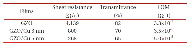
Table 2 shows the optical and electrical properties of the films. The GZO/Cu films had a lower sheet resistance compared to that of the GZO single layer films. The figure of merit (FOM) is an important index for evaluating the performance of transparent conducting oxide (TCO) films [13]. The FOM is defined as FOM=T10/Rs, where T is the optical transmittance and Rs is the sheet resistance. Although the optical transmittance of GZO films is deteriorated with the Cu bottom layer, GZO/Cu films have the one order lower sheet resistance compared to that of the GZO single layer films. Thus, the FOM reached a maximum of 5.0×10⁻⁵Ω-1 for the GZO 100 nm/Cu 5 nm films, which is greater than the FOM for the GZO single layer films and the In2O3 films prepared in a previous study [14]. It is supposed that the enormous electrons in the Cu bottom layer may enhance the carrier density and enhance the electrical properties of the GZO/Cu films. Since the higher FOM value indicates better quality of TCO films, it is supposed that the GZO films with 5 nm thick Cu bottom layers will likely perform better in TCO applications than GZO single layer films.
[Table 2.] The comparison of figure of merit (FOM,Ω-1).

The comparison of figure of merit (FOM,Ω-1).
Both GZO and GZO/Cu bi-layered films were deposited on glass substrates using RF and DC magnetron sputtering. The optical and electrical properties were dependent on the Cu bottom layer in the GZO/Cu films.
Figure of merit for the GZO 100 nm/Cu 5 nm films reached a maximum value of 4.3×10⁻⁵Ω-1, which was greater than that of the GZO single layer films. This result indicates that the 5 nm thick Cu bottom layer in the GZO/Cu films results in better performance compared to conventional GZO single layer films.