Transparent conductive oxide (TCO) layers play a very important role in today’s optoelectronic devices such as liquid crystal displays (LCDs), organic light emitting devices (OLEDs) and plasma display panels (PDPs). Among the most widely used TCO materials, tin-doped indium oxide thin films have drawn significant attention because of their well-known physical properties such as low resistivity and high transmittance in the visible wavelength region [1,5-7]. In order to grow high-quality ITO film, various deposition processes have been reported, including the RF/DC magnetron sputtering, chemical vapor deposition (CVD) and pulsed laser deposition (PLD) methods [9-13]. Among the technologies available for ITO thin film production, magnetron sputtering has the advantage of being able to produce films with good quality [8]. In addition, the sputtering technique is frequently used due to its good reproducibility, high deposition rate and good adhesion of the coatings to the substrate [3]. Recently, the preparation of high quality ITO films on plastic substrates is in great demand regarding applications for flexible display devices. However, characteristic properties of the film on polymer substrates are not easy to improve since the substrate heating is limited due to weak thermal resistance [5].
In this study, initially ZnO film as a buffer layer was deposited on glass substrate prior to ITO film deposition in order to improve crystallinity and film property of ITO and then subsequent deposition of ITO film was made on ZnO/glass by RF magnetron sputtering at 150℃. The structural, electrical and optical properties of Glass/ZnO/ITO film were systematically investigated in term of different film thickness regarding the ZnO buffer layer. In order to estimate and compare with the experimental results, the simulation program, the Essential Macleod program (EMP), was adopted.
ITO and ZnO thin films were prepared by RF magnetron sputtering at 150℃. The compositions of the ITO target consisted of 90 wt.% In2O3 and 10 wt.% SnO2. The ZnO film was deposited on glass substrate at a sputtering thickness ranging from 0 to 125 nm. Subsequently, the ITO film was deposited at sputtering
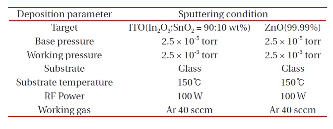
[Table 1.] Deposition parameters for ZnO buffer and ITO film by RF magnetron sputtering.

Deposition parameters for ZnO buffer and ITO film by RF magnetron sputtering.
thickness of 35 nm. The sputtering chamber was evacuated to 2.5 × 10⁻⁵ Torr before sputtering. The pressure during deposition was 2.5 × 10⁻³ Torr. Mass flow controlled pure argon (99.999%) was delivered to the chamber at a flux of 40 sccm. The substrate to target distance was 8 cm. The RF power was set to 100 W. Prior to deposition, the target was pre-sputtered for 15 min in order to remove any contamination. The deposition conditions of the samples are shown in Table 1.
For optical characterization, the EMP was adopted and the calculated results were compared with measured optical properties [4]. The simulation with variable parameters such as wavelength (400-700 nm) and thickness of layers [Glass/ZnO/ITO] was designed.
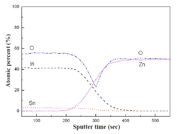
The thickness of the ITO layer was fixed at 35 nm and that of the ZnO buffer layer was varied between 0 and 125 nm, as determined by the Alpha-step. The crystal structure of the films was analyzed by X-ray diffraction. The electrical properties of the films were obtained using a four-point probe method. The optical transmission spectra were measured in the wavelength ranging from 400-700 nm by a spectrophotometer. In addition, the interfacial properties of the optimized Glass/ZnO(100 nm)/ ITO(35 nm) electrodes were analyzed using AES depth profiling.
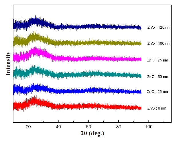
Figure 1 shows XRD patterns of the ITO film and ZnO buffer layers deposited with various ZnO thicknesses (0, 25, 50, 75, 100, 125 nm) at 150℃. All the films deposited at 150℃ showed that no characteristic diffraction peak of ITO was identified and only the amorphous nature of glass substrate was observed. It is believed that all films were shown to be amorphous because their grain
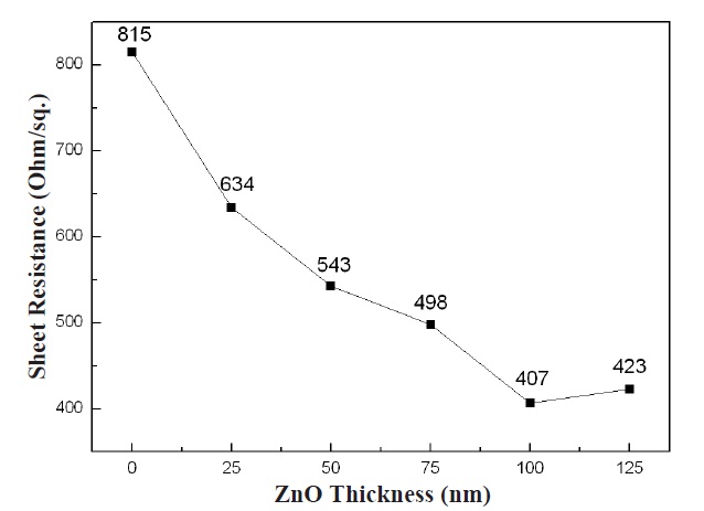
[Fig. 2.] Sheet resistances of ITO thin films with different film thickness of the ZnO buffer layer.
sizes were too small to detect the characteristic diffraction peak by the X-ray diffraction (XRD) method.
Figure 2 shows the sheet resistance of the ITO films deposited at 150℃. The sheet resistance of single ITO film with a thickness of 35 nm was approximately 815 Ω/sq. because of the low substrate temperature. The sheet resistance of the ITO films decreased with increasing thickness of the ZnO buffer layer. However, ZnO buffer layers thicker than 100 nm resulted in an increase of sheet resistance. In the case of the ITO film, the lowest sheet resistance of 407 Ω/sq. was obtained at a ZnO buffer layer thickness of 100 nm. It is believed that the crystallinity of ITO was improved such as the characteristic properties due to the insertion of the ZnO buffer layer.
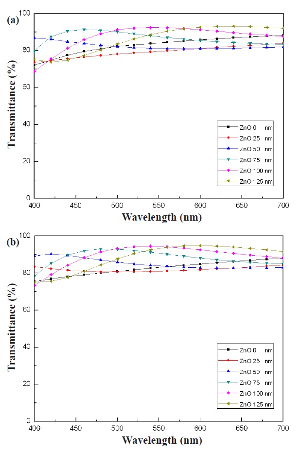
Figure 3(a) shows the simulation results for the optical transmittance on the glass/ZnO/ITO multilayer film as a function of the ZnO thickness. The optical simulation was carried out by means of an EMP. All ITO films had high transmittance (>80%) in the visible light region. The multilayer film with the thickness of glass/ZnO(100 nm)/ITO(35 nm) exhibits the highest optical transmittance of 92% at 550 nm. The transmittance of glass/ ZnO/ITO multilayer films was higher than that of single layer ITO films.
Figure 3(b) shows the measured optical transmittance of the glass/ZnO/ITO multilayer films as a function of the ZnO thickness. Similar to the simulated optical transmittance result, the transmittance spectra have shown that all films exhibit high transmittance (>80%) in the 400-700 nm range. The multilayer film with the thickness of glass/ZnO(100 nm)/ITO(35 nm) exhibits the highest optical transmittance of 92% at 550nm. The transmittance of glass/ZnO/ITO multilayer films was higher than that of single layer ITO films. It is believed that the transmittance was increased with the increasing film adhesion property due to the insertion of the ZnO buffer layer.
In transparent conductor applications, electrical and optical coating parameter optimization plays a key role. Both conductivity and transmittance should be as high as possible for TCO applications. Hence the optimum value for these two parameters should be established using figure of merit. The most commonly used definition for figure of merit ΦTC regarding a transparent conducting film was first given by Haacke [2] as:
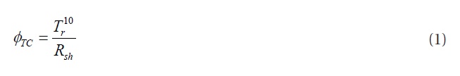
where
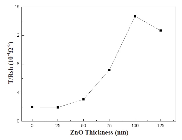
Rsh the sheet resistance. Figure 4 shows the calculated figure of merit (ΦTC). It was shown that the ΦTC value of the glass/ZnO/ITO multilayer film was increased from 2×10⁻⁴Ω-1 to 14.7×10⁻⁴Ω-1 by increasing the film thickness of the ZnO buffer layer. However, ZnO buffer layers thicker than 100 nm resulted in a decrease for figure of merit
Figure 5 shows the AES depth profiles of the optimized glass/
ZnO(100 nm)/ITO(35 nm) electrodes on the glass substrate. Even the individual ITO and ZnO layers are well and clearly defined, some interdiffusion behavior can be observed between ITO film and the ZnO buffer layer.
ITO films were prepared on glass substrates using an RF magnetron sputtering method at 150℃. According to XRD results, the structure of glass/ZnO/ITO multilayer film showing no characteristic diffraction peak of ITO was identified and only the amorphous nature of glass substrate was observed. However, the electrical and optical properties of ITO films were significantly improved through insertion of a ZnO buffer layer between the ITO film and glass substrate. The sheet resistance of the films decreased from 815 Ω/sq. to 407 Ω/sq. and optical transmittance increased from 82% to 92% at a wavelength of 550 nm when a 100 nm ZnO buffer layer was deposited. We believe glass/ZnO/ ITO multilayer film showed satisfactory properties for applications such as transparent conducting electrodes.