The Microstructure and nonlinear electrical properties of the ZPCCYT (ZnO-Pr6O11-CoO-Cr2O3-Y2O3-Tb4O7) varistors were investigated for different amounts of Tb4O7. The addition of Tb4O7 has a significant effect on microstructure and electrical properties. Analysis of the microstructure indicated that the ceramics consisted of ZnO grain as a main phase and a few secondary phases as a mix of Pr6O11, Y2O3, and Tb4O7. As the amount of Tb4O7 increased, the sintered densities of pellets increased from ρ = 5.70 to 5.78 g/cm3 and the average grain size decreased from d = 4.8 to 3.6 μm. The increase in the amount of Tb4O7 increased from EB = 7,473 to 10,035 V/cm and from α = 39.7 to 52.2. In particular, it was found that the ceramics modified with 1.0 mol% in the amount of Tb4O7 are suited for the varistors for high voltage in the light of a high sintered density and a high voltage gradient.
Modern electronic systems are constantly growing toward that of high speed and multifunction. Furthermore, they are more complex with higher levels of integration. As a result, they are very sensitive to transient voltage and eventually, may be destroyed by internal or external surges. Therefore, they should be protected from bizarre overvoltage in order to have credible reliability. ZnO varistors are ceramic semiconductor devices, which are manufactured by sintering zinc oxide added with various subordinate oxides, such as Pr6O11, CoO, Cr2O3, etc. They are called multijunction grain boundary devices because they have a large number of unit structures of semiconductiong ZnO graininsulating intergranular layer- semiconductiong ZnO grain like a back-to-back Zener diode in a three-dimensional series-parallel network. ZnO-based varistor ceramics exhibit voltage-switching properties at a critical value in accordance with increasing voltage. Voltage-switching properties enable ZnO varistors to be used widely in the field of overvoltage protection systems from electronic circuits to electric power systems [1-4].
ZnO-Pr6O11-based varistor ceramics have been studied to further enhance the varistor properties [5-11]. Nahm et al. reported that Zn-Pr-Co-Cr (ZPCC)-Rare earth oxide (R = Er, Y, Dy, etc.)-based varistor ceramics have highly nonlinear properties and high stability against various stresses [12-22]. These varistor ceramics are based on 5 components in ceramic composition. In order to develop the varistor ceramics of high performance and wide band applications, it is very important to comprehend the effects of the additives on nonlinear properties. Thus far, no study on the effects of Tb4O7 on the electrical properties and stability of ZnO-Pr6O11-based varistor ceramics consisting of 6 components has been reported. In this work, the microstructure and electrical properties of the ZPCCYT (ZnO-Pr6O11-CoO-Cr2O3- Y2O3-Tb4O7) were systematically investigated.
Reagent-grade raw materials were used in the proportion of (97.5-x) mol% ZnO, 0.5 mol% Pr6O11, 1.0 mol% CoO, 0.5 mol% Cr2O3, 0.5 mol% Y2O3, x mol% Tb4O7 (x = 0.25, 0.5, 0.75. 1.0). Raw materials were mixed by ball milling with zirconia balls and acetone in a polypropylene bottle for 24 h. The mixture was dried at 120℃ for 12 h and calcined in air at 750℃ for 2 h. The calcined mixture was pulverized using an agate mortar/pestle and after the addition of 2 wt% polyvinyl alcohol (PVA) binder, granulated by sieving through a 100-mesh screen to produce the starting powder. The powder was uniaxially pressed into a disk-shaped pellet of 10 mm in diameter and 2 mm in thickness at a pressure of 80 MPa. The pellets were sintered for 1 h at 1,300℃ and furnace-cooled to room temperature. The heating and cooling rates were 4 ℃/min. The sintered samples were lapped and polished to 1.0 mm thickness. The final samples were roughly 8 mm in diameter and 1.0 mm in thickness. Silver paste was coated on both faces of the samples and the electrodes were formed by heating at 600℃ for 10 min. The electrodes were 5 mm in diameter. Finally, after soldering the lead wire to both electrodes, the samples were packaged by dipping them into a thermoplastic resin powder.
2.2 Microstructure examination
Both surfaces of the sintered pellets were lapped and ground with SiC paper and polished with 0.3 μm-Al2O3 powders to a mirror-like surface. The polished samples were thermally etched at 1,100℃ for 30 min. The surface microstructure was examined by a scanning electron microscope (SEM, Hitachi S2400, Japan). The average grain size (d) was determined by the lineal intercept method, given by d=1.56 L/MN, where L is the random line length on the micrograph, M is the magnification of the micrograph, and N is the number of the grain boundaries intercepted by the lines [23]. The compositional analysis for minor phases was carried out by an energy dispersion X-ray spectroscope (EDS) attached to the SEM unit. The crystalline phases were identified by an X-ray diffractometry (XRD, Rigaku D/max 2100, Japan) with CuKα radiation. The sintered densities (ρ) of the pellets were measured using a density determination kit (238490) attached to a balance (AG 245, Mettler Toledo International Inc., Greifensee, Switzerland).
The electric field-current density (E-J) characteristics were measured using a V-I source (Keithley 237). The breakdown field (EB) was measured at 1.0 mA/cm2 and the leakage current density (JL) was measured at 0.8 EB. In addition, the nonlinear coefficient (α) is defined by the empirical law, J = K·Eα, where J is the current density, E is the applied electric field, and K is a constant. The α was determined by the following expression [24] α = (logJ2-logJ1)/ (logE2-logE1), where J1 = 1.0 mA/cm2 and J2 = 10 mA/cm2, E1 and E2 are the electric fields corresponding to J1 and J2, respectively.
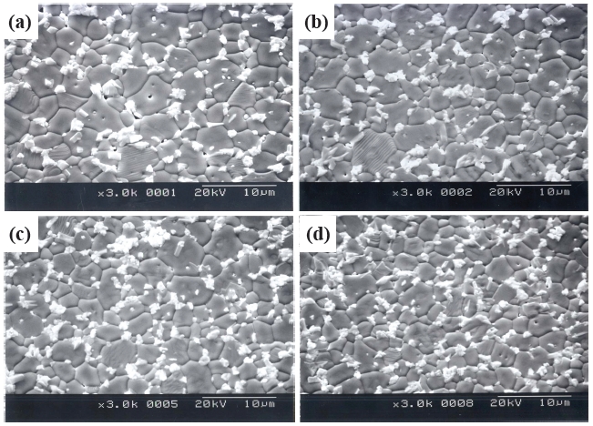
Figure 1 shows the SEM micrographs of the samples for different amounts of Tb4O7 . By observing intuitively, the microstructure of the samples consisted of ZnO grain (black in the color) as a primary phase and an intergranular layer (white in the color) as a secondary phase. The average grain size (d) decreased from 4.8 to 3.6 μm (see Fig. 5 in advance) and it was very uniformly distributed. The sintered densities (ρ) of pellets increased from 5.70 to 5.78 g/cm3 (5.78g/cm3 in pure ZnO) with an increase in the amount of Tb4O7 (see Fig. 5 in advance) and they were very densified with almost zero porosity. These ceramics were noticeably improved in terms of the densification and the uniformity of
grain size in the microstructure, compared with ZPCCY ceramics sintered at 1,350℃ not 1,300℃, with no Tb4O7 [14].
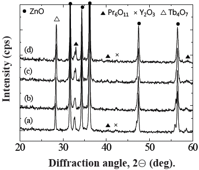
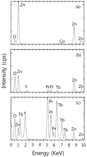
Figure 2 shows the XRD patterns for different amounts of Tb4O7 . The microstructural phases consisted of ZnO grain as a main phase and an intergranular layer as secondary phases. It was confirmed that the intergranular layer was a mix of Pr6O11, Y2O3, and Tb4O7 -rich phases. It was found from EDS indicated in Fig. 3 that the Pr6O11, Y2O3, and Tb4O7 are segregated at grain boundaries and nodal points due to an ionic radius difference for Zn, and coexist in the grain boundaries and the nodal points as if they were a single phase. The detailed microstructural parameters are summarized in Table 1.
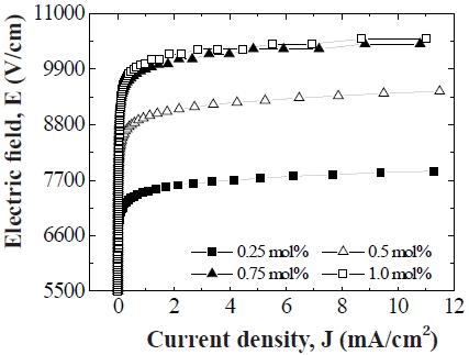
Figure 4 shows the E-J characteristics of the samples for different amounts of Tb4O7. The most important characteristics of the varistor ceramics are that the electrical conduction exhibits piecewise linear relation, which divides into a linear region with very high impedance and a nonlinear region with very low impedance. In a linear E-J relation, the predominant conduction mechanism is a thermionic emission over the Shottky potential barrier before the critical operation field (EB). In a nonlinear E-J relation, the predominant conduction mechanism is a Fowler- Nordheim field emission (tunneling) through a Shottky potential barrier. These nonlinear properties are attributed to the distinctive microstructural feature, in which the grain boundaries between ZnO grains are active and as a result, the Schottky potential barrier exists.
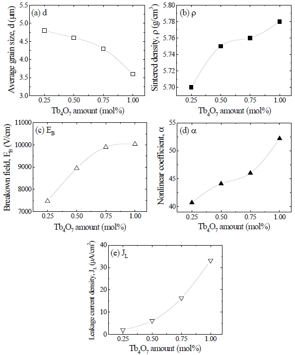
The behavior of the breakdown field (EB) as a function of an amount of Tb4O7 was indicated graphically in Fig. 5(c). The EB

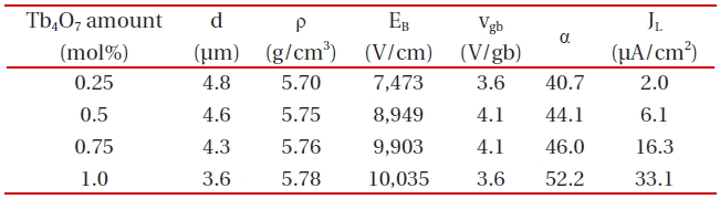
Average grain size (d), sintered density (ρ), breakdown field (EB), breakdown voltage per grain boundary (vgb), nonlinear coefficient (α), and leakage current density (JL) of the samples for different amounts of Tb4O7 .
increased noticeably from 7,473 to 10,035 V/cm with an increase in the amount of Tb4O7 [14]. The sample added with 1.0 mol% Tb4O7 is a very high breakdown field above 10,000 V/cm. Obviously, this will contribute to the manufacturing of the compact ZnO element. The EB is predominantly controlled by the grain size (d), and slightly depends on the breakdown voltage per grain boundaries (vgb). The breakdown voltage (VB) is indicated as the following expression [1,2] VB = (D/d)·vgb = n·vgb, furthermore, the EB is written as follows: EB = vgb/d, where d is the average grain size, D is the thickness of the sample, and n is the number of grain boundaries. Therefore, the VB is proportional to n and vgb. In general, to control the breakdown voltage, one is to control the sample thickness for fixed grain size or alternately one is to
control the grain size for constant sample thickness. As a result, the increase of EB with an increase in the amount of Tb4O7 is attributed to the decrease of the average ZnO grain size and the decrease of breakdown voltage per grain boundaries.
The behavior of the nonlinear coefficient (α) as a function of an amount of Tb4O7 was indicated graphically in Fig. 5(d). The α of the samples increased remarkably from 39.7 to 52.2 with an increase in the amount of Tb4O7 . In the vicinity of the knee of curves, the α depends on the ratio of thermionic emission and Fowler-Nordheim field emission in the Shottky potential barrier. That is, the α will absolutely increase if the Fowler-Nordheim field emission is much more predominant than the thermionic emission [24].
The behavior of leakage current density (JL) as a function of sintering temperature was indicated graphically in Fig. 5(e). The JL increased remarkably from 2.0 to 33.1 μA/cm2 with an increase in the amount of Tb4O7 . The leakage current in the electric field region below the breakdown field is due to the thermionic emission over the Schottky barrier. Therefore, the higher barrier height leads to the higher α and consequently the lower leakage current. However, the experimental results obtained in this study are completely different from other general cases. It is assumed that the reason why the leakage current increases with increasing α is attributed to an increase of the recombination current between electrons and holes in the vicinity of the grain boundaries [25].
The effect of Tb4O7 on the microstructure and electrical properties of ZPCCYT varistor ceramics was investigated for different amounts of Tb4O7. The microstructure consisted of ZnO grain and intergranular phases containing Pr6O11, Y2O3, and Tb4O7. The incorporation of Tb4O7 improved the sintered densities of pellets and uniform grain size. The addition of Tb4O7 has a significant effect on electrical properties such as: an increase in the breakdown field, nonlinear coefficient, and leakage current. On the contrary, the increase in the amount of Tb4O7 caused the leakage current to increase. These ceramics could be applied to the varistors for high voltage of a compact type, with a high sintered density above 98% of theoretical density and a high breakdown field greater than 7,000 V/cm.