After Geim and Novoselov’s research in 2004 [2], graphene has come to be regarded as a highly promising material in a variety of areas on account of its mechanical, optical, electrical, physical, thermal, and chemical properties. Graphene is known to consist of carbon atoms with a two-dimension and hexagonal phase in a crystal lattice; it is classified as a carbon allotrope with zero-dimension fullerenes, one-dimension nanotubes, and three-dimension graphite [3]. Like a synthetic fiber, graphene has led to research trends in a lot of research groups and many researchers has carried out considerable studies regarding not only fundamental experiments but also commercial applications [4]. Consequently, graphene synthesis techniques, such as the mechanical exfoliation technique [5], chemical vapor deposition (CVD) growth [6,7], chemical exfoliation of graphite [8], and epitaxial growth on SiC [9] have been investigated systematically. For electrical and chemical applications in particular, CVD growth is mainly employed; this synthesis technique produces high quality, large area, and continuous graphene films as compared with other techniques. Moreover, graphene has been introduced into multifarious applications in various fields, such as transparent electrodes [10], flexible and stretchable electronics [11,12], heat transport [13], super-capacitors [14], sensors [15], barriers [16], field effect transistors [17], and composites [18].
CVD graphene utilizes various gases as carbon sources, such as methane, ethylene, and acetylene; hydrogen is used as an etching reagent, one that can reduce defective structures by regulating the growth rate. Recently, CVD graphene using liquid precursors has been reported and found to have advantages due to its low cost and easy, simple, and safe handling. Miyata et al. [19] studied graphene synthesis using ethanol on nickel foil under atmospheric pressure with Ar; a mono layer and a few layers of graphene using nhexane were also prepared under low pressure with Ar/H2 [20]. Besides this, CVD graphene growth processes using ethanol and pentane under atmospheric pressure on copper foil [21], and using methanol, ethanol, and propanol under low pressure [22] have been reported. However, most of the studies mentioned above reported only restrictively about the growth method and electrical devices, without detailed study of the synthesis.
Herein, we report on a parametric study of CVD graphene growth using methanol as a carbon source under low pressure. Since methanol is the only precursor, it was possible to optimize the growth conditions of the graphene by controlling only two parameters, such as pressure and temperature at high temperature; methanol is easily decomposed into hydrocarbon and water (etching reagent) [1], so an additional etching reagent is not necessary. The D/G ratio, which is related to the defect density of graphene, is found to decrease with increasing temperature and decreasing pressure. The electrical conductivity of graphene, on the other hand, is found to increase with increasing temperature and pressure. Also, we found that the crystallinity of graphene and the number of layers were affected by growth temperature and pressure. The optical transmittance of graphene was also investigated at various temperature conditions (700℃ through 1000℃) in order to approximately calculate the number of graphene layers [23]. In order to accurately estimate the number of graphene layers, transmission electron microscope (TEM) analysis was performed for the same samples.
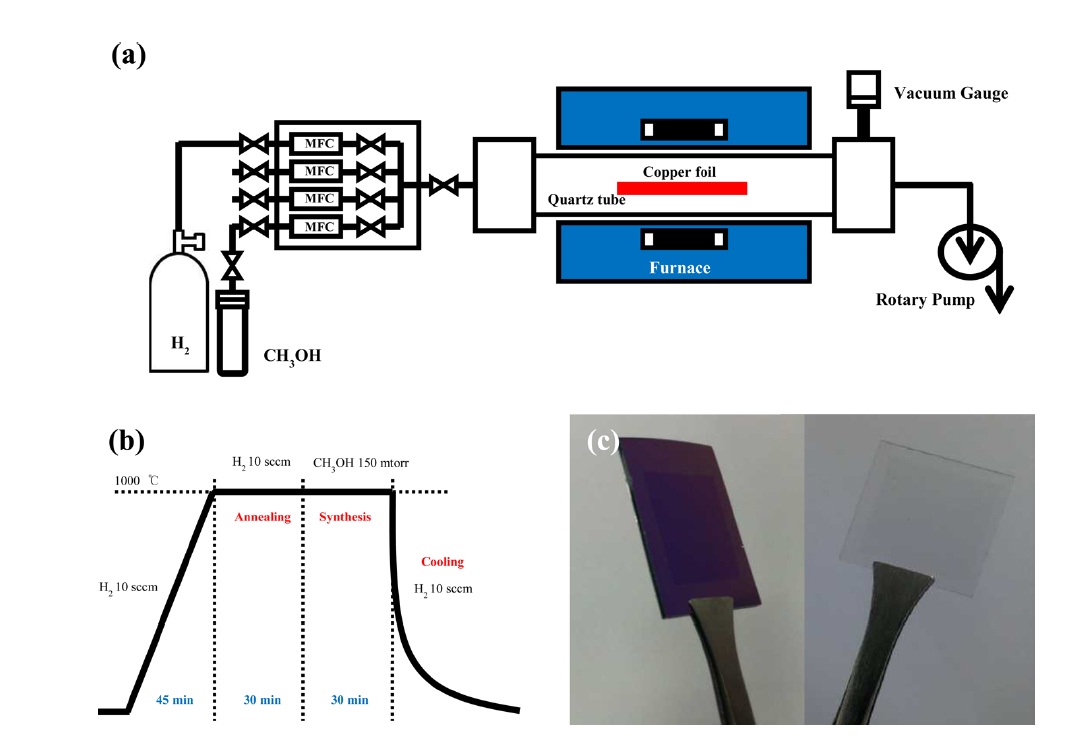
2.1. Graphene synthesis method
The CVD system for graphene growth was kept under low pressure CVD (LPCVD). The methanol solution was used as a carbon source. A thin copper foil (25 μm thick) provided from Alfa Aesar was used as a transition metal catalyst substrate. The thin copper foil was located at the middle position in a 2 inch quartz tube in the CVD device; we operated a rotary vacuum pump that was used in order to maintain low pressure. The temperature of the CVD furnace was increased to 1000℃ for approximately 45 min. The pressure of the hydrogen was 53 mtorr and the flow rate was 10 sccm. Subsequently, in order to develop larger grain boundaries and a smooth surface, the sample was annealed at 1000℃ for 30 min under the same hydrogen atmosphere. Then, a carbon source was introduced into the quartz tube furnace for the nucleation and growth of graphene. The amount of carbon source was controlled using a mass flow controller (MFC) connected to a methanol containing glass component. During the synthesis, hydrogen gas was completely stopped, and the pressure was approximately 150-155 mtorr. The temperature was changed from 700℃ to 1000℃ in order to investigate the effect of temperature on the graphene quality. After the synthesis, the carbon source was completely stopped and the quartz tube was cooled down using 10 sccm of hydrogen gas.
Graphene on the thin copper foil was transferred to various substrates for Raman spectroscope and atomic force microscope (AFM) analysis; it was transferred to TEM grids for TEM analysis. The spin coating using poly methyl methacrylate (PMMA) on graphene/thin copper foil was carried out at 4200 rpm for 40 s, followed by heating of the graphene/thin copper foil at 180℃ for 1 min. Then, ammonium persulfate [(NH4)2S2O8] dissolved in water was used in order to separate and remove the thin copper foil. The film of PMMA/graphene was rinsed at least three times using deionized water for 20 min. Subsequently, the PMMA/graphene film was transferred onto a 300 nm SiO2/Si substrate and glass substrate. PMMA on graphene was then removed with acetone.
As-grown graphene films on the thin copper foil were analyzed using a scanning electron microscope (SEM) instrument (S-4700, Hitachi); the transferred graphene on the 300 nm SiO2/ Si substrate was analyzed by Raman spectroscopy (Horiba) and AFM (Veeco Dimension 3100). The optical transmittance was measured with UV-Vis spectroscopy (Jasco V-670). The sheet resistivity was measured using a four-point-probe resistivity meter (FPP-RS, DASOL ENG). TEM (JEM-2200FS), equipped with beam electron diffraction, was used to analyze the structure and the number of graphene layers.
Fig. 1a provides a schematic diagram of the LPCVD. Methanol as a liquid carbon source was stored in a glass component in which the temperature was maintained at 30℃ water and methanol vapor was introduced into a quartz tube furnace using the MFC, which allows a precise control of a carbon source. Thin copper foil was used as a catalyst substrate due to the low solubility of carbon atoms [7]; thus, nucleation and growth of graphene can occur via surface adsorption of carbon atoms [24]. After the graphene growth, the graphene/copper foil was transferred, using a typical method [25], to various substrates, such as a 300 nm SiO2/Si substrate and a glass substrate, as shown in Fig. 1c. The optical transmittance of graphene is too high to be clearly observed at the location of graphene on the substrates, as shown in Fig. 1c. Considering the good optical and electronic properties of graphene, CVD graphene films can be used in transparent and flexible electrodes [10].
Fig. 2 shows a data set collected from the methanol CVD graphene films under the optimized conditions. An SEM image of the as-grown graphene film is shown in Fig. 2a; graphene covered a large area of the thin copper foil over grain boundaries. Besides this, wrinkles and ripples of graphene can be identified on the copper surface due to the different thermal expansion coefficients between the copper and the graphene [26]. Some particle-like impurities were also found to exist on the graphene surface because evaporated copper re-deposited at the growth temperature.
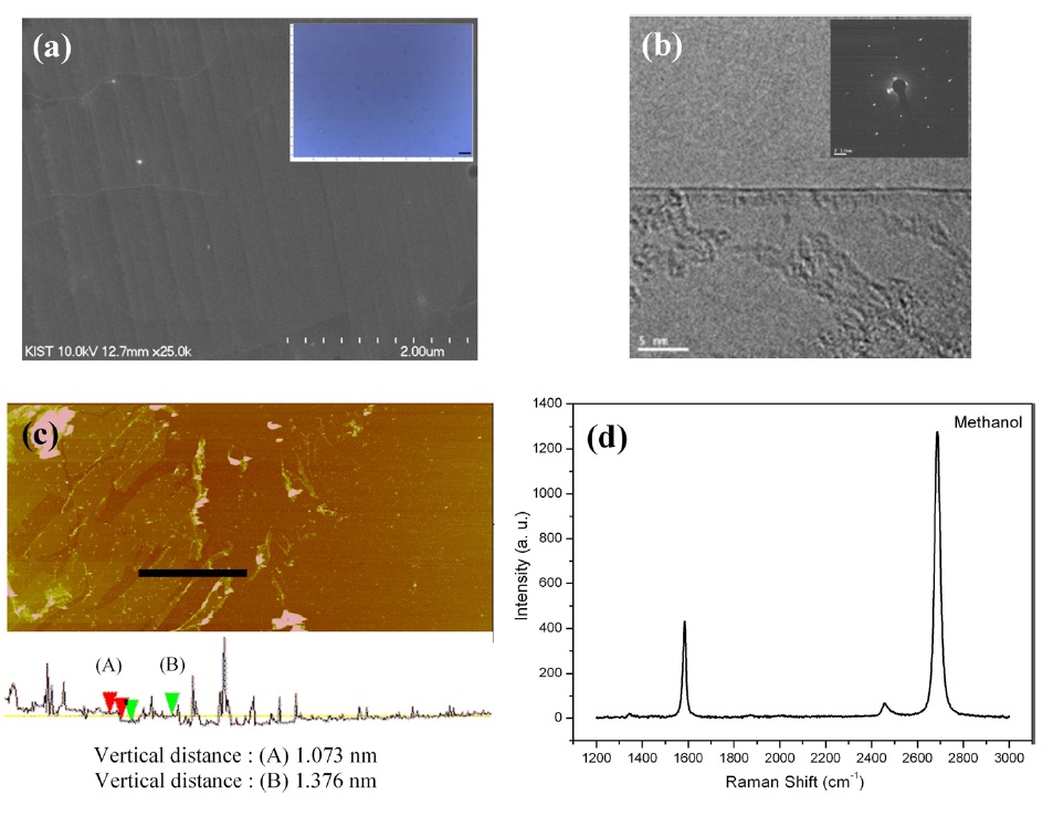
The inset in Fig. 2a shows an optical image of a graphene
film transferred to a 300 nm SiO2/Si substrate; the scale bar in the image is 2.5 μm. A large area of the graphene was easily transferred to other substrates without causing serious damage.
A monolayer of graphene film can be seen in the TEM image in Fig. 2b. The inset in Fig. 2b shows selected area electron diffraction (SAED) data, which indicate that the methanol CVD
graphene films have good crystallinity, showing clear hexagonal structures. AFM was used to analyze the thickness and the morphology of graphene films. The vertical distances were 1.073 nm and 1.376 nm at the two different spots. These values correspond to 1-2 layers, considering AFM measurement errors and the fact that the interspace between graphite layers is approximately 0.4 nm.
Fig. 2d shows the Raman spectrum of the graphene films. In the Raman spectrum, the D peak represents defects or disorder in the structure; the G peak represents the tangential mode of the graphitic structures [27]. The intensity of the G' peak represents the second order of the zone-boundary phonons [28]. These peaks can be seen at 1344 cm-1 (D), 1585.7 cm-1 (G), and 2687.9 cm-1 (G'). Graphene quality and number of layers can be estimated from the D/G and G′/G (2D/G) ratios of the Raman spectrum. Ferrari et al. [29] reported that the G′/G (2D/G) ratio of monolayer graphene obtained using the procedure of micromechanical cleavage of graphite showed a figure of roughly 4; also, the full width at half maximum (FWHM) was about 25 cm-1. However, the G′/G (2D/G) ratio of monolayer CVD graphene showed a value of more than 2; the FWHM was 33 cm-1 [7]. In this experiment, the D/G ratio and G′/G ratio of the methanol CVD graphene were 0.04 and 2.95, respectively; the FWHM was 30.4 cm-1. Considering the TEM, Raman, SEM, and AFM data collected from the methanol CVD graphene, it seems that methanol as a carbon source can be effectively transformed to large area and high quality graphene films without using an etching reagent because methanol itself can be decomposed promptly to hydrocarbon and water (etching reagent) at high temperatures [1]. Thus, in comparison with methane CVD gra-phene [7] and mechanically exfoliated graphene [29], methanol CVD graphene showed competitive characteristics.
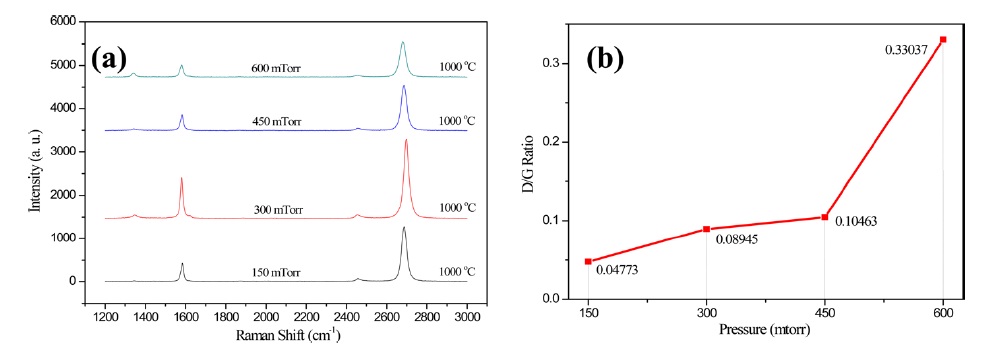
In order to investigate the effect of pressure on the crystallinity and the quality of graphene, the pressure of CVD synthesis was changed from 150 mtorr to 600 mtorr with 150 mtorr. The grown graphene films were analyzed using Raman spectroscopy after transfer of the graphene films onto a SiO2/Si substrate. As shown in Fig. 3a and b, the D/G ratio tended to increase with the increasing pressure. Li et al. [30] reported that the nucleation density of graphene under low pressure was lower than that of graphene under high pressure, and thus the lower nucleation density of graphene led to a significant increase in the size of the single crystalline domain in methane CVD growth. It appears that the tendency of the D/G ratio observed in our samples was similar to that in the previous study. The higher nucleation density at a higher pressure led to frequent formation of domain boundaries, which formed defects in hexagonal structures. The other reason for the high nucleation density could be amorphous carbon formation in the graphene structures due to the limited catalytic activity of the Cu foil with the increased methanol flux. Our results confirmed that methanol CVD graphene films grown under the lowest pressure had good quality and crystallinity with a minimal degree of defects or disorder.
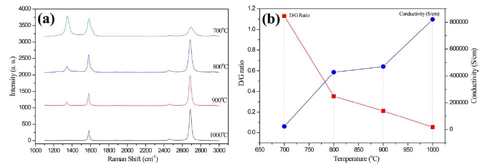
Defects and disorder in graphene could be affected not only by the pressure but also by the temperature. In order to investigate the temperature effect, the pressure was kept at 150 mtorr for all the synthesis experiments; the synthesis temperature was varied from 700℃ to 1000℃ at intervals 100℃ . As illustrated in Fig. 4a and b, the intensity of the D peak increased with decreasing temperature. Accordingly, both the D/G ratio and the
electrical conductivity of methanol CVD graphene decreased with decreasing temperature. The defects and disorder in the crystalline lattices negatively affected the conductivity. Thus, these results prove that the temperature was one of the most important parameters for the growth of highly crystalline and good quality methanol CVD graphene films.
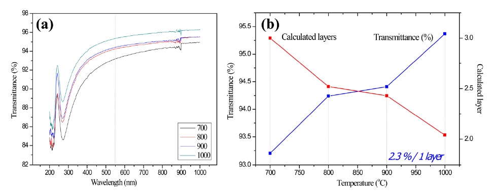
We further investigated the UV-Vis spectra of methanol CVD graphene film grown under various temperature conditions. As shown in Fig. 5a, the optical transmittance was measured in order to determine the number of layers. The number of graphene layers was calculated by considering that 2.3% absorption corresponded to one layer [23]. In other words, 95.3% of the optical transmittance shown in Fig. 5b could be calculated as representing approximately 2 layers of the methanol CVD graphene.
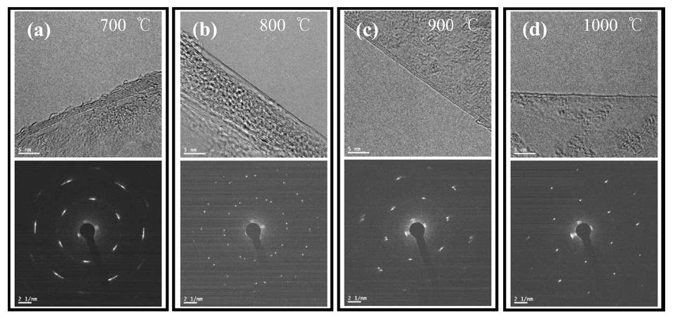
High resolution TEM (HR-TEM) images were collected in order to precisely estimate the number of layers and to compare that estimation with the optical transmittance data. The number of graphene layers was commonly counted at the folded edge of the graphene. As shown in Fig. 6d, monolayer graphene films were frequently observed at 1000℃, which is the highest temperature in our experiments. In addition, SAED, as can be seen in Fig. 6d, showed hexagonal patterns that represent a highly crystalline structure. On the other hand, the HR-TEM images in Figs. 6a-c show that double-, triple-, or multi-layers of methanol CVD graphene were grown under those conditions. These results correspond with the optical transmittance data, shown in Fig. 5b. This tendency was also observed in carbon nanotube CVD growth, such that high quality single-walled carbon nanotubes were grown at the higher temperatures while defective multi-walled carbon nanotubes were grown at the lower temperatures [31].
Graphene growth using a methanol CVD method was parametrically studied. The optimized conditions were reached when graphene films were grown under 150 mtorr pressure and at a temperature of 1000℃ for a fixed growth time. Hydrocarbon and water decomposed from the methanol at high temperatures were used as a carbon source and as an etching reagent for graphene growth. The D/G ratio of the methanol CVD graphene decreased in accordance with increasing temperature and decreasing pressure. On the contrary, the electrical conductivity of the methanol CVD graphene increased proportionally with increasing temperature and decreasing pressure. The pressure and temperature for graphene growth affected the number of layers and the crystallinity of the graphene. Considering the various results collected from SEM, Raman, AFM, TEM, UV-Vis, and four-point-probe measurement, the quality of methanol CVD graphene was found to be comparable to that of methane CVD graphene and graphene formed under mechanical exfoliation. Thus, the methanol CVD graphene growth described here was a cheap, safe, easy, and simple method for continuous, high quality, and large area graphene synthesis.