Since the launch of Korean Institute of Technology Satellite (KITSAT)-1, interest in studying the behavior of electronic devices in space radiation has increased (Shin et al. 1999, Kim et al. 2004). There was an attempt made to monitor the space radiation environment using radiation-sensitive field effect transistor (RADFET) (Kim et al. 2006) as a total dose indicator. Subsequent studies and experiments also included single-event effects, using proton beam facilities (Lim et al. 2006, Ryu et al. 2007). As heavy ion facilities are not yet available in Korea, the ground tests of single-event effects are restricted to using proton beam line. In the development of satellites, radiation characteristics were modeled based on the measured values using foreign facilities (Baek et al. 2001). This has limited the independent development of space-qualified electronic devices.
As the amount of data collected increases, current and future satellites require more and more memory space for their various missions. A synchronous dynamic random access memory (SDRAM) mass memory unit (MMU) has been developed for use in satellite systems for future applications that require high-speed data processing and large data storage (Langley & Murray 2004). Recently, we developed a SDRAM MMU using a domestic memory core. The SDRAM MMU is composed of a Samsung double data rate 2 (DDR2) SDRAM (K4T1G164QE) package of 1 Gbit that can be stacked up to 4 Gbit. In order to investigate the radiation characteristics of the mass memory, single event effect (SEE) experiments were performed using the Heavy Ion Medical Accelerator in Chiba (HIMAC, Japan).
A large number of protons and other heavy ions exist in space, and the mechanisms by which SEE occur are known to be different for protons and heavy ions. The protons can generate SEE through spallation, while heavy ions generate SEE through direct ionization. Even though the number density of the heavy ions is quite lower than that of protons, the heavy ions are more abundant in the larger linear energy transfer (LET) that are proportional to the charge amount collected by the direct ionization. Consequently, independent experiments using protons and heavy ions are required in order to correctly specify the behavior of microelectronics in space radiation environments.
The SEE characteristics of the SDRAM chip were investigated using the HIMAC medium energy beam line, and have LET values ranging up to ~70 MeVcm2/mg for Si as the target material with various heavy ion species of C, Si, Ar, Fe, Kr, and Xe. The device under test (DUT) showed single-bit upset (SBU), multi-bit upset (MBU), and single-event functional interrupt (SEFI) when exposed to the ion beam. However, single-event latch-up (SEL) was not observed during the exposures.
In Sections 2 and 3, a detailed overview of the test and its results are introduced with statistical analyses. It is anticipated that the results of the SEE experiments will provide guidelines that explain the evolution of the SEE characteristics of current and future memory devices, which can be used in space missions, as nano technologies are adopted in the manufacturing processes.
2. EXPERIMENT PROCEDURE AND CONDITION
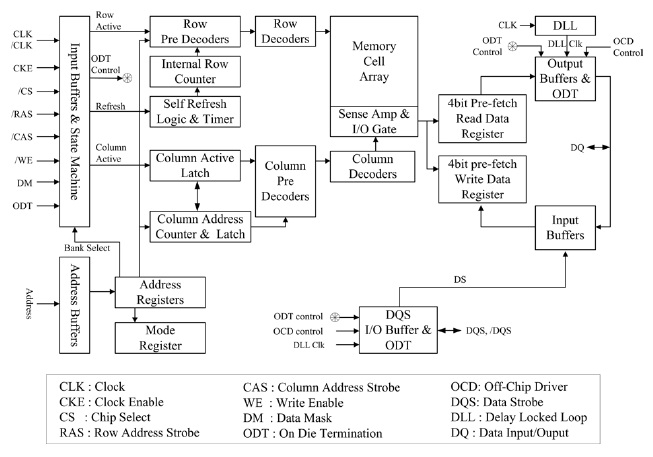
Test was conducted on 1 Gbit DDR2 SDRAMs (K4T1G164QE) for investigation of SEE characteristics. DDR2 SDRAM has a double-data-rate synchronous dynamic random-access memory interface, which allows a higher bus speed and requires lower power. Fig. 1 shows the functional block diagram of a DDR2 SDRAM. The key features of the K4T1G164QE are as follows:
- Manufacturer: Samsung
- Type: DDR2 SDRAM
- Technology 56 nm complementary metal-oxide-semiconductor (CMOS)
- Density: 1 Gbit
- VDD = VDDQ = 1.8V ± 0.1V
- Clock frequency: 333 MHz for 667 Mb/sec/pin, 400 MHz for 800 Mb/sec/pin
- Internal banks: 8 banks
- Bit organization: 16
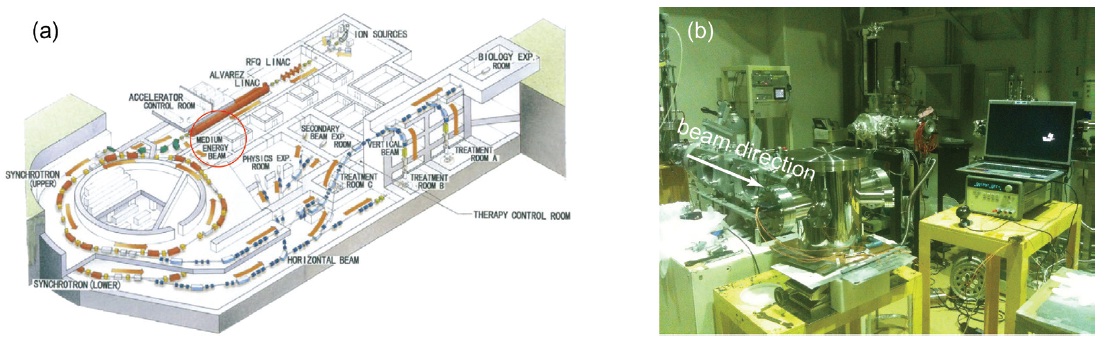
The experiment was performed using the medium beam line of the HIMAC synchrotron, depicted as a red circle in
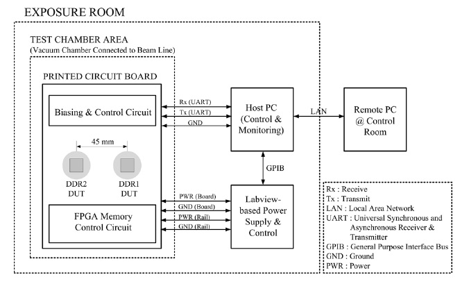
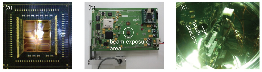
Fig. 2a (Murakami et al. 2008). Fig. 2b shows the vacuum chamber, in which the DUT is mounted and connected to the beam nozzle and SDRAM control laptop. Instead of the de-capsulation process, the DUT (DDR2 SDRAM) was fabricated without an epoxy molding compound molding process, as shown in Fig. 3a. The SDRAM chip has a size of 6.0 × 7.1 mm and was mounted on a printed circuit board (PCB) that has field-programmable gate array (FPGA) controller electronics and a related circuit that monitors the function and status of the memory chip during the exposures. The PCB was carefully designed so that all the electronics except the SDRAM were located outside the beam line, as shown in Fig. 3b. The SDRAM was mounted within the diameter of the HIMAC heavy ion beam line, which has a uniform distribution with ~3 cm beam diameter. The PCB was mounted in a vacuum chamber, as shown in Fig. 3c; the vacuum chamber is directly connected to the beam line output and is controlled by a laptop through the vacuum feed-through.
The electrical configuration devised for the experiment is depicted in Fig. 4. The power supply provided the required voltage and current to the PCB, where the values were controlled and monitored by the laptop through a GPIB/USB connector. Then, the host PC was connected to the remote control PC through a LAN connection between the exposure room and control room. The overall test procedure presented by Schwank et al. (2008) was adopted for these experiments.
During the exposure, the SEU and SEL were monitored using real-time communication with the on-board FPGA chip via an interface cable connected to the control laptop. Initially, the content of the memory was written with a fixed pattern of ‘0101010101010101’ and the memory cells were scanned during the exposure in order to monitor the
single event upset (SEU) event. If the content of the memory changed, the FPGA sensed the change and reported it to the control computer via the interface channel. For the single event latch-up monitoring, the change in the current input to the memory chip was monitored. If the current change exceeded the criteria (~1.2 times the usual current value), it was regarded as SEL, and the chip was autonomously reset in real time as suggested by Schwank et al. (2008). However, SEL events did not occur during the experiment.
We performed the experiment according to the following procedure.
a) Mount a vacuum chamber to the 6 MeV/u LINAC beam line
b) Mount PCB and focus the beam position to DDR2 SDRAM
c) Close the vacuum chamber and pump out (~10-5 Torr)
d) Beam line on and measure SEU and SEL. Specific beam exposure times were determined in situ, based on the initial short time exposure and total fluence according to the atomic species.
e) Run the self-monitoring (SEU, SEFI, & SEL) algorithm from the remote control room and operate the gate of the beam for the specified duration, then check the results.
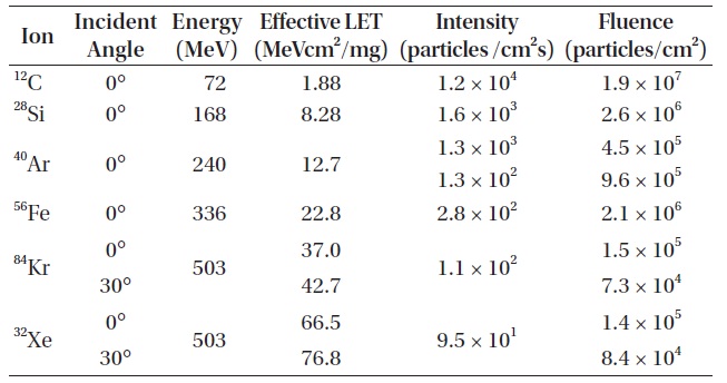
The parameters of the heavy ion beam used in the experiment are listed in Table 1. As shown in the table, six ion species including 12C, 28Si, 40Ar, 56Fe, 84Kr, and 132Xe were engaged in the experiment. The medium beam line of the HIMAC provides fixed beam energy of 6 MeV per atomic mass, and the corresponding effective LETs ranged from
[Table 1.] The heavy ion beam parameters of HIMAC, used in the SEE experiments.

The heavy ion beam parameters of HIMAC, used in the SEE experiments.
1.88 to 66.5 MeVcm2/mg. We prepared three identical test boards and changed the test boards after exposing to two species in series so that the experiments were not affected by total ionizing dose. The incident angle was varied by 30° for 84Kr and 132Xe to evenly extend the LET range as shown in Table 1. For each species, the intensity was measured using a secondary electron emission monitor and CR-39 before the main exposure. The beam profile was also measured using a GAF film to check the beam uniformity. Then, it was determined that the exposure time was not affected by the total ionizing dose. The fluence was adjusted from ~105 to ~107 particles/cm2 in order to secure a statistically-meaningful numbers of events for each ion species. For 40Ar, the intensity of the beam was varied ten times in order to determine whether there were dependencies on the beam intensity. The heavy ion beam provided by HIMAC was a pulse beam with a fixed spill period of 1.65 s and a spill width of 5 μs.
During the experiment, several different behaviors were observed that were caused by the heavy ion precipitation. First, SBUs (classified as SEUs) were observed in all ion species. MBUs, mostly between two neighboring bits, were observed for LET values larger than 37 MeVcm2/mg. For the SEFI, the different behaviors were categorized as ‘halt,’ ‘control logic error,’ or ‘stuck bit recoverable by power reset.’ When the memory chip did not respond with symptoms of the current increase, it was considered to be a halt and the exposure was stopped. These halts occurred in heavy ions with LETs larger than 12.7 MeVcm2/mg. A bit flip in a critical control register can result in an SEFI. In summary, the radiation characteristics of the SDRAM under heavy ion bombardment could be categorized as follows.
● SEU
◆ SBU: temporary change of information in a cell that can be recovered by memory recycling.
◆ MBU: temporary change of information in multiple cells that can be recovered by memory recycling.
● SEL: halt of memory function with abrupt increase of current that can be recovered only by power reset (not observed in this experiment.)
● SEFI: temporary malfunction of memory that can be recovered by mode register reset or power reset.
◆ Halt: halt of memory function without evident increase of current.
◆ Control address logic error: SEU-like behavior in correlated or patterned address of several to hundreds of cells that can be ascribed to a single-event upset error in the address control logic rather than in memory cells.
◆ Stuck bit: semi-permanent change of bit information that can be recovered by power reset or annealing.
A series of false upsets were observed in an area of physically or logically related cells, which cannot be explained using the flipped cell information. The addresses of the flipped information, which are presented as burst errors in other research (Koga et al. 2002, Ladbury et al. 2006), could be more than 1,000 while the number of related addresses is random in nature. In this case, the memory is recovered in the next rewriting cycle. Furthermore, stuck bits, which are specific bits that cannot be written as commanded, were observed in two different behaviors during the exposures. One type of stuck bit could be cleared with a power reset; this type of soft error is classified as an SEFI following the previous description of the phenomena (Koga et al. 2007). In some cases, the stuck bits continued after the power reset. These were observed when the DUT was exposed to heavy ions whose LETs were larger than 22 MeVcm2/mg. In all cases, the stuck bits disappeared within several hours during the functional tests in a vacuum that were waiting for changes in the ion species. However, it could not be confirmed that the stuck bits were related to the total ionizing dose, as was noted by Henson et al. (1999)
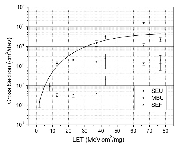
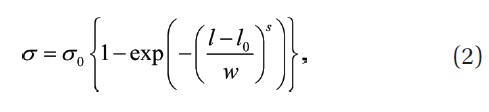
Fig. 5 shows the cross-section values of the SEU, MBU, and SEFI according to the effective LETs. The cross-section for the given LET, σ (LET), was derived from the relationship between the number of SEE occurrences, N, and the fluence, f (LET), and is given as follows:
The error ranges for cross-section values were also deduced according to Poisson statistics, and marked as error bars in the graph. The statistical distribution that is used to describe the failure behavior of a population of identical components, each of which can fail independently, and all of which must function for the device, is the Weibull distribution (Petersen et al. 1992). It has been used to describe the heavy ion SEE cross-section curve. The SEU cross-section was fitted with the Weibull function as follows:
where
Compared with the previous technologies that have been fabricated in 90 nm CMOS technology nodes (Ladbury et al. 2006), the SEU and MBU do not show increasing trends, while the SEFI is somewhat increased. Instead, the LET threshold (
SEE experiments were performed in order to investigate the radiation characteristics of the DDR2 SDRAM (K4T1G164QE) fabricated in 56 nm technology, using the HIMAC heavy ion accelerator facility. The cross-section values for SEU, MBU, and SEFI were derived up to ~80 MeVcm2/mg. A comparison of the proposed DDR2 SDRAM with the previous technologies implies that the increased degree of integration in the fabrication causes the radiation performance to become vulnerable to SEFI but resistant to SEL up to an LET of ~80 MeVcm2/mg.
Even though the experiments were performed using a foreign facility, this research is significant as the first Korean SEE experiment using a domestic semiconductor chip. More studies on the mechanism that causes this tendency are suggested for future research; an additional experiment to observe the radiation behavior in high-energy protons is also planned.