This paper proposes a novel scheme of a gray scale fingerprint image for a high-accuracy capacitive sensor chip. The conventional grayscale image scheme uses a digital-to-analog converter (DAC) of a large-scale layout or charge-pump circuit with high power consumption and complexity by a global clock signal. A modified capacitive detection circuit for the charge sharing scheme is proposed, which uses a down literal circuit (DLC) with a floating-gate metal-oxide semiconductor transistor (FGMOS) based on a neuron model. The detection circuit is designed and simulated in a 3.3 V, 0.35 ㎛ standard CMOS process. Because the proposed circuit does not need a comparator and peripheral circuits, the pixel layout size can be reduced and the image resolution can be improved.
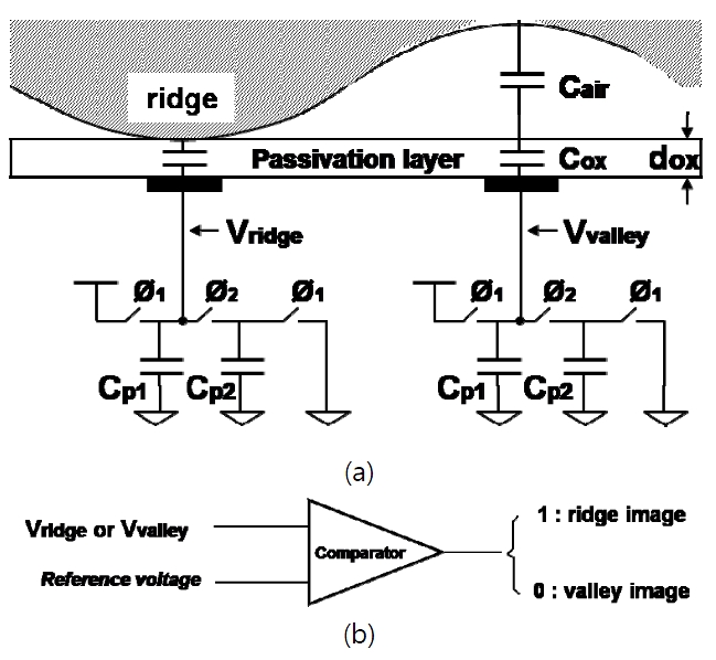
A capacitive fingerprint sensor uses a capacitive sensor array to detect fingerprints. The name ‘capacitive’ comes from the fact that the finger skin and the sensor electrode produce a capacitor whose capacitance is determined by the distance from the chip surface to the finger skin. The finger is modeled as the upper electrode of the capacitor, and the metal plate in the sensor cell as the lower electrode as shown in Fig. 1. These two electrodes are separated by the passivation layer of the silicon chip and air. Cox has a fixed capacitance which is determined by the passivation-layer thickness dox and the relative dielectric constant εox. Cair however, has a variable capacitance according to the distance dair. The series-connected capacitor Cf is composed of a capacitor between the metal plate and the chip surface and another one between the chip surface and the finger skin. The capacitance of Cf is at its maximum value when a ridge has contact with the passivation layer. As the distance between the chip surface and the finger’s skin increases, the capacitance becomes smaller. The variation of capacitance is transferred to the output voltage by the sensing scheme.
The comparator discriminates a ridge and valley by reference voltage as shown in Fig. 1b [1, 2]. A reference voltage compares the voltage from the sensor and the fingerprint’s ridge and valley to create a binary image. A gray scale fingerprint image is needed for more accurate processing of a fingerprint algorithm. Some circuits have been designed to obtain a gray scale image in semiconductor fingerprint sensors [3]. However, these results require a complex module such as a digital-to-analog converter (DAC) and a large scale layout. This paper proposes a novel scheme of a gray scale fingerprint image for a high-accuracy capacitive sensor chip.
In this paper, we describe the conventional sensing scheme using a charge pump circuit in section II. The concept and design result of the proposed sensing scheme is described in section III.
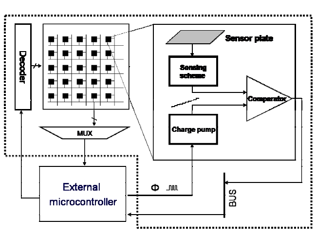
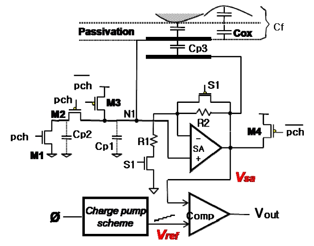
Fig. 2 shows a typical fingerprint sensor block diagram with a charge pump for the gray scale image [3]. This method swings a reference voltage from 0 V to Vdd. On a finger contact, the charge pump circuit receives a clock from the microcontroller to increase the comparator’s reference voltage.
The comparator compares fingerprint’s sensing voltage and charge pump circuit’s output voltage, which acts as a reference voltage. It then saves a number of the clock at the point in which the logic is changed from 0 to 1. When the value of each pixel is saved in memory, it is a gray scale image value in each pixel.
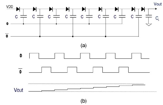
Fig. 3 shows the charge pump circuit and timing diagram.In general, a charge pump circuit is applied as a voltage multiplier for the nonvolatile memory. Due to the two non-overlapping clock signals, the voltage gradually increases. One stage is composed of one diode and an actual coupling capacitor. As an effect of the diode, the voltage is transferred in only one direction, to show an overall gradual output voltage increase effect.
Fig. 4 shows the detail sensing circuit and timing diagram with a charge pump in the sensor pixel level. SA is a simple analog buffer of differential input. With the beginning of the unit-gain mode, the S1 is low and R1 and R2 do not operate. The SA is enabled as a unit-gain buffer and tracks the voltage change of the node N1, which nulls when the potential difference between the two electrodes of Cp3 is zero. Therefore, SA can effectively remove the influence of Cp3. In the sensing mode, S1 is high and SA operates as an attenuator. Immediately after the unit-gain mode, the effect of Cp3 is removed by the unit-gain buffer. The final sensing voltage will be between a ridge and valley voltage without the influence of the parasitic capacitance Cp3. The charge pump circuit receives a clock from the microcontroller to increase the comparator’s reference voltage. The comparator compares the fingerprint’s sensing voltage and charge pump circuit’s output voltage, which acts as a reference voltage.
The above method is effective for gray level sensor design without a DAC. However, it requires a global clock-controlled charge pump in each pixel. The conventional gray scale image scheme uses a DAC with a large layout or a charge-pump circuit with high power consumption and circuit complexity by a global clock signal. A modified capacitive detection circuit of the charge sharing scheme is proposed, which uses a down literal circuit (DLC) with a floating-gate MOS (FGMOS) based on a neuron model.
>
A. Floating-gate MOS Transistor (FG MOSFET)
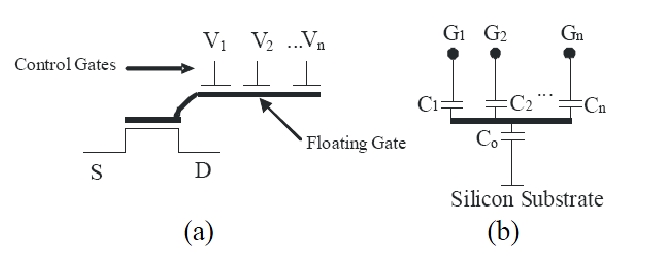
FGMOSFETs (which use two poly silicon layers) are widely used as digital memory because they have long-term charge retention that makes them non-volatile devices, conveniently storing the desired information [4]. Plenty of literature can be found related to the diverse applications of FGMOSFETs in items such as neural networks, instrumentation electronics, and soft-hardware logic (SHL). The name "neuron MOS" (νMOS) is used when it is designed with one or more control gates since it simulates the operation of a biological neuron [5]. Due to its multiple inputs, the corresponding signals are added at the floating gate and the transistor will be either on or off depending on the sum value. The symbol of this device is shown in Fig 1a. It can be seen that the floating gate has no electrical connection since it is completely surrounded with silicon dioxide. Fig. 1b shows the equivalent circuit of a FGMOSFET multiple input gate, represented by a voltage divider formed with capacitors. From this circuit, it is easily shown that the floating gate voltage is a weighted sum of the voltages applied on the control gates. The floating gate voltage can be found with the following expression:
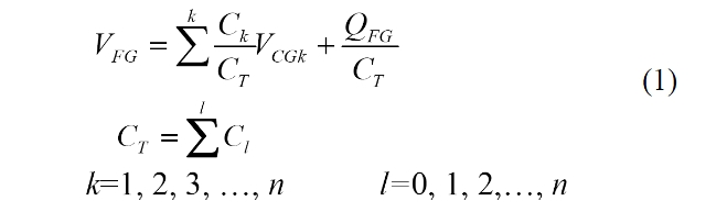
where VFG is the floating gate voltage, C0 is the gate capacitance, Ck are the control gate capacitances, QFG is the charge present over the floating gate and n is the number of control gates of the neuron MOS. Thus, the floating gate voltage depends both on the voltage applied over the control gates and any charge that could be present at the floating gate.
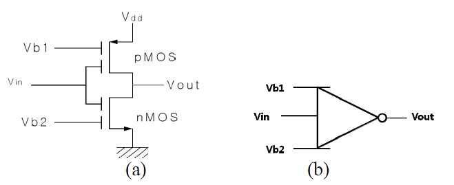
The application of FGMOS circuitry leads to reduced gate complexity and, thus, to low power design on the circuit level. A voltage-mode FGMOS down literal circuit that realizes an arbitrary down literal function is shown in Fig. 6. It provides the benefit that the circuit can be easily fabricated by the standard CMOS process, instead of the multi-level ion implantation applied in the conventional circuit. It has a variable threshold voltage VTC by way of controlling only two bias voltages as shown in equation (2) [6]. This means obtaining a different output Vout from the same input Vin. Its noise margin and switching sensitivity are greater than those of the variable-threshold C-VMOS inverter presented by Shibata.
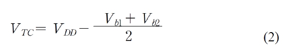
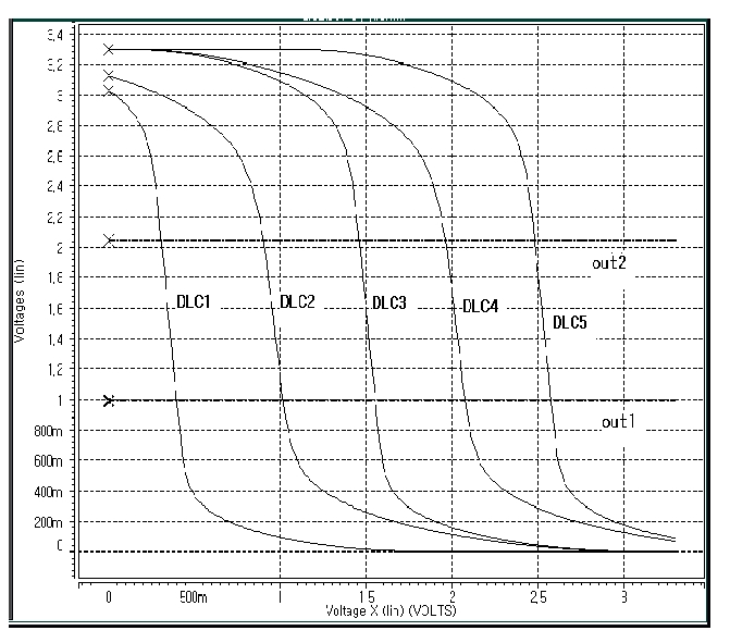
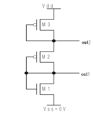
Fig. 7 shows the simple reference voltage circuit to provide Vb1, Vb2 and by optimization of the reference circuit MOS M1, M2, and M3, if out2 is about 2 V and out1 is 1 V, we can obtain the VTC of the DLC with various bias voltages as shown in Table 1.
[Table 1.] VTC of down literal circuit with various bias voltages (Vdd = 3 V)
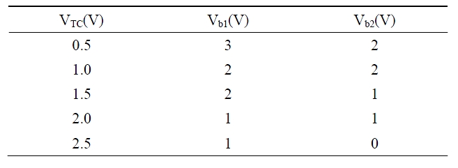
VTC of down literal circuit with various bias voltages (Vdd = 3 V)
>
C. Design of Novel Sensing Circuit with DLC
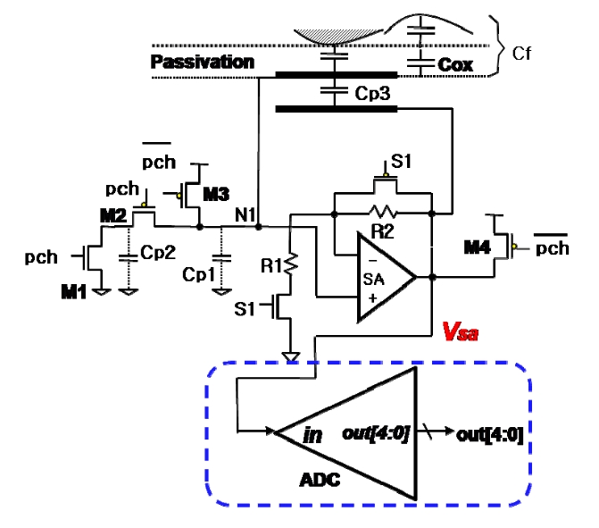
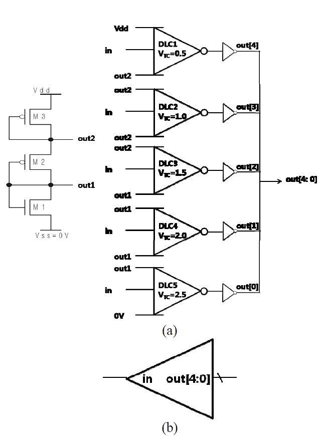
Fig. 8 shows the proposed analog-to-digital converter (ADC) circuit for converting a sensing signal to 6-level gray scale digital output. It is composed of the reference circuit and 5 DLCs. The 5 DLCs have 5 logic threshold voltages, 0.5 V to 2.5 V. Each output of the DLCs is connected to normal inverter gate for full swing from Vdd to 0 V.
Fig. 9 shows the result of dc analysis for VTC in DLC with various bias voltages. The VTC of DLC1 is about 350 mV because of its power mismatch and FGMOS optimization, but the influence of the DLC0 VTC difference is not dominant for obtaining a gray scale in our sensing circuit. Out1 and out2 are the output of the reference voltage circuit. Fig. 10 shows the proposed sensing circuit with a 6-level gray image using ADC with DLC. The circuit does not need the comparator of Fig. 4. This means a reduction of gate count complexity and power consumption as well as gray scale image output.
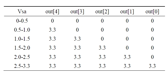
Output of analog-to-digital converter for various input range of sensing voltage (Vdd = 3.3 V)
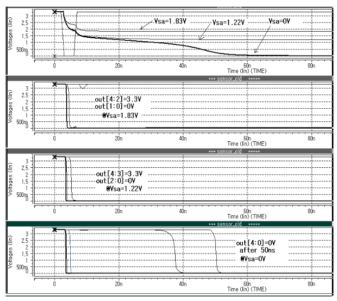
We also expect the improvement of the sensor chip image resolution through the reduction of the unit pixel layout area. Table 1 shows the output of ADC for various values in the input range of the sensing voltage. Fig. 11 shows the simulation result of the proposed sensing circuit, Vdd = 3.3 V 0.35 ㎛ CMOS typical parameter. The result shows that the proposed sensing circuit performs a valid function for a 6-level gray scale image. When the Vsa is 1.83 V at a ridge, out [4:2] is logic high and out [1:0] is logic low. When the Vsa is 1.22 V between a ridge and valley, out [4:3] is logic high and out [2:0] is logic low. When the Vsa is 0 V at a valley, out [4:0] is logic high after 50 ns.
This paper describes the possibility of a low-power, high-resolution fingerprint sensor chip for a gray scale image output using the DLC of a FGMOS. The application of FGMOS circuitry leads to reduced gate complexity and, thus, to low power design on the circuit level. The conventional gray scale image scheme uses a DAC with a large layout or a charge-pump circuit with high power consumption and complexity by a global clock signal. A modified capacitive detection circuit with a charge sharing scheme, which uses DLC with a FGMOS based on a neuron model, is proposed. The proposed ADC circuit converts a sensing signal to a 6-level gray scale digital output. It is composed of the reference circuit and 5 DLCs. The 5 DLCs have 5 logic threshold voltages, 0.5 V to 2.5 V. Each output of the DLCs is connected to a normal inverter gate for the full swing from Vdd to 0 V. Because the proposed circuit does not need the comparator and peripheral circuits of a conventional circuit, the pixel layout size can be reduced and the image resolution can be improved. This means the reduction of the gate count complexity and power consumption as well as gray scale image output. We also expect the improvement of the sensor chip image resolution through the reduction of the unit pixel layout area. The detection circuit was designed and simulated in a 3.3 V, 0.35 ㎛ standard CMOS process. The result shows that the proposed sensing circuit performs a valid function for a 6-level gray scale image.