Wireless communication has been developed rapidly in the past decades and it already has a great impact on human life. In the field of wireless communications, antennas play a vitally important role. In the late 1970s, there was rapid development in the field of microstrip patch antenna technology. In early 1980s, antenna elements and arrays were developed in terms of design and modeling. Due to their advantages like light weight, reduced size, low cost, conformability, and the ease of integration with an active device, these antennas have been extensively studied. A microstrip patch antenna is the combination of a radiating patch on one side of the dielectric substrate and ground on the other side. The patch is generally made of a conducting material like gold or copper. The radiating patch and the feed lines are usually photo etched on the dielectric substrate. Microstrip patch antennas radiate primarily because of the fringing fields between the patch edge and the ground plane. Therefore, the antenna can be fed by a variety of methods. These methods can be classified into two categories: contacting and non-contacting. In the contacting method, the radio frequency (RF) power is fed directly to the radiating patch using a connecting element such as a microstrip line or probe feed. In the non-contracting method, electromagnetic field coupling is performed to transfer power between the microstrip line and the radiating patch which includes proximity feeding and aperture feeding [1, 2].
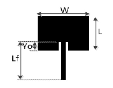
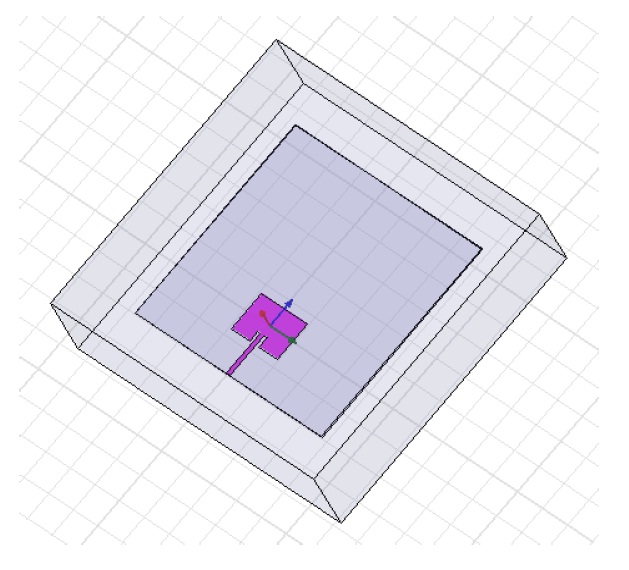
Microstrip antennas are characterized by a large number of physical parameters. They are designed to have many geometrical shapes and dimensions but rectangular and circular microstrip patches have been used in many applications. In this paper, the design of an inset feed rectangular microstrip patch antenna at 2.45 GHz for wireless communication is presented having length L, patch width W, inset fed distance Yo, and transmission line length Lf, as shown in Fig. 1. This antenna is designed on flame retardant 4 (FR-4) substrate and its performance characteristics, which include return loss, voltage standing wave ratio (VSWR), gain, and radiation pattern, were obtained from a simulation.
II. ANTENNA GEOMETERY AND ITS DESIGN REQUIREMENTS
For a rectangular patch, the length L of the patch is usually 0.333
There are three essential parameters for the design of an inset fed rectangular patch antenna. They are resonant frequency (fr), dielectric material of the substrate (εr), and the thickness of the substrate. The resonant frequency selected for this design is 2.45 GHz.
The dielectric material of the substrate selected for this design is FR-4, which has a dielectric constant of the 4.7 and a loss tangent equal to 0.019. The dielectric constant of the substrate material is an important design parameter. A low dielectric constant of the substrate material is used in the prototype design because it gives better efficiency, a higher bandwidth, and a low quality factor Q. The low value of the dielectric constant increases the radiated power. The design has a patch size independent of the dielectric constant. Therefore, the reduction in the patch size is accomplished by using a higher dielectric constant and FR-4 is good in this agreement. The small loss tangent was neglected in the simulation.
The thickness of the substrate is another important design parameter. The thickness of the substrate increases the fringing field at the patch periphery like the low dielectric constant and increases the radiated power. The height of the dielectric substrate of the inset microstrip patch antenna is h = 1.6 mm.
III. MATHEMATICAL CALCULATION OF THE ANTENNA PARAMETERS
The parameters of the antenna can be calculated by the transmission line method.
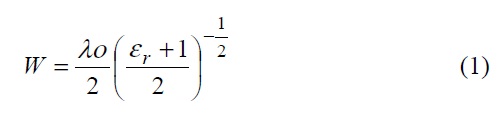
The width of the antenna can be determined by
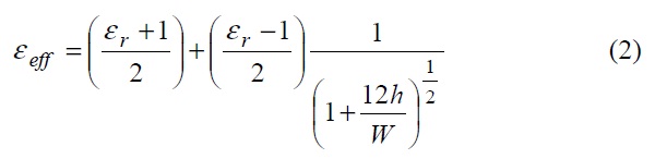
The effective constant can be obtained by
where
ε
ε
The dimensions of the patch along its length have n ow been extended on each end by a distance
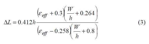
The actual length L of the patch is given by
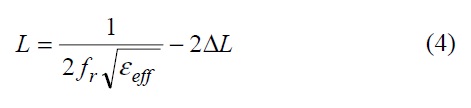
Where
The inset feed introduces a physical notch, which in turn introduces a junction capacitance. The physical notch and its corresponding junction capacitance influence the resonance frequency. As the inset feed-point moves from the edge toward the center of the patch, the resonant input impedance decreases monotonically and reaches zero at the center. When the value of the inset feed point approaches the center of the patch,
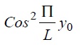
where
IV. SIMULATION AND MEASUREMENT RESULTS
The antenna was simulated in high frequency structure simulator (HFSS), which is a high performance full-wave electromagnetic (EM) field simulator for arbitrary 3D volumetric passive devices, with a Microsoft Windows graphical user interface. The antenna designed in the HFSS simulator is shown in Fig. 2.
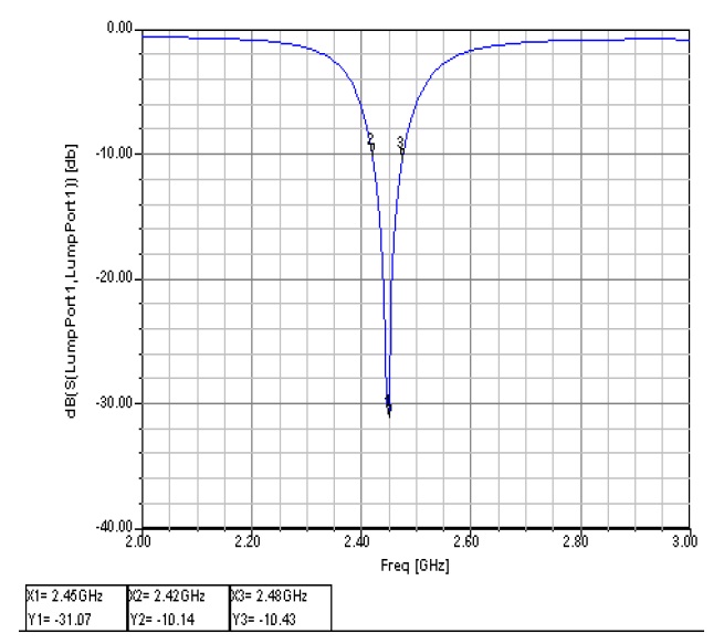
The simulated return loss of the inset-fed antenna is - 31.07 dB at the center frequency of 2.45 GHz as shown in Fig. 3.
The bandwidth of the antenna as a percentage is defined by
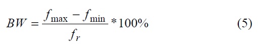
where
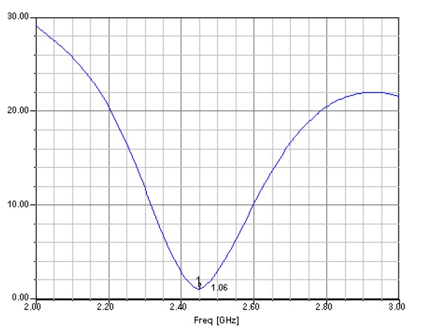
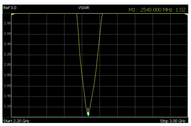
The VSWR characteristic of the antenna should fall in between 1 and 2. From simulation, its value is 1.06 at 2.45 GHz as depicted in Fig. 4.
Also, the radiation pattern of the antenna obtained is shown in Fig. 5 at phi = 90 degrees (red) and phi = 0 degrees (blue) at 2.45 GHz. This shows the gain of the antenna is 3.408 dB.
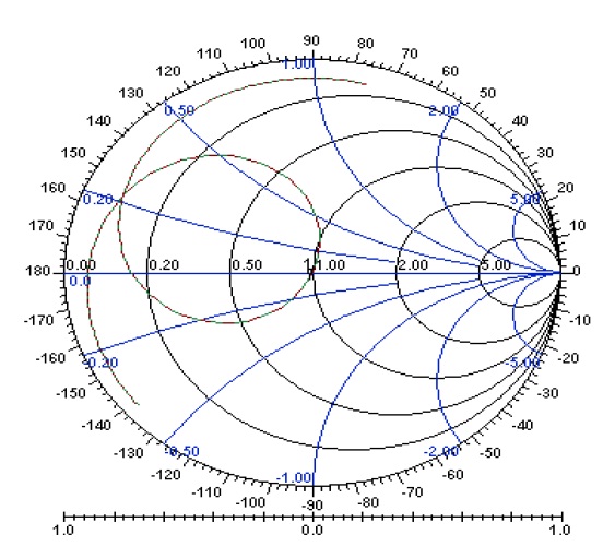
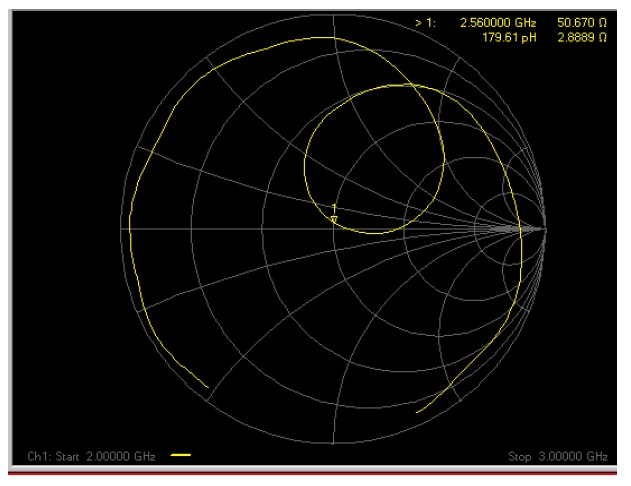
The scattering parameter for the antenna design at 2.45 GHz is shown in the Smith chart in Fig. 6.
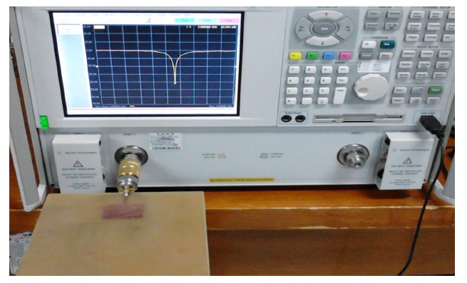
The inset fed microstrip patch antenna is fabricated on a FR-4 printed circuit board (PCB) and the measurement setup is done by using an Agilent Technologies (Santa Clara, CA, USA) N5230A 10 MHz - 40 GHz PNA-L-Network Analyzer as shown in Fig. 7.
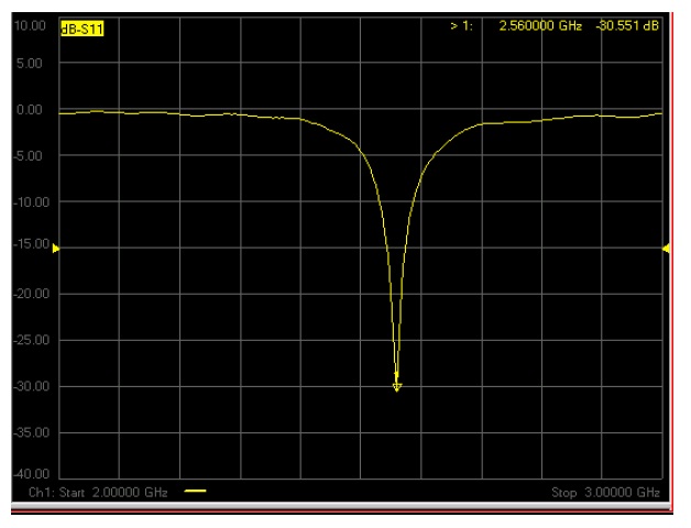
The measured return loss is obtained to be -30.551 dB at 2.56 GHz as shown in Fig. 8 and impedance match at 50 Ω is shown in Fig. 9. The VWSR was measured with an Agilent Technologies N9912A found to be 1.02 at 2.548 GHz as shown in Fig. 10.
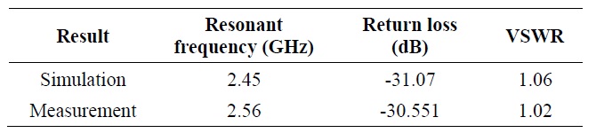
The resonant frequency shifted from the designed frequency of 2.45 GHz. The reason for the shift may be due to the FR4 board. In the physical design of the antenna, a material having varying εr, length, width, and thickness of the board may cause shifting of the resonant frequency. Other factors may also have an effect, such as the chemical used in etching accuracy and the surface finish. The difference between the simulated and fabricated measured value is shown in Table 1.
[Table 1.] Comparison between simulation and fabricated measured results

Comparison between simulation and fabricated measured results
In this paper, the mathematical calculation for design of an inset rectangular patch antenna at 2.45 GHz is presented. The simulation of an inset-fed microstrip patch antenna was performed in HFSS. The antenna performance characteristics such as return loss, VSWR, gain, and radiation pattern were obtained in the simulation. The fabricated antenna frequency was compared with the simulated resonance frequency. It was found to be slightly different than the simulated value as real world physical parameters may not be exactly the same.