A 1 GHz CMOS fast-lock phase-locked loop (PLL) is proposed to support the quick wake-up time of mobile consumer electronic devices. The proposed fast-lock PLL consists of a conventional charge-pump PLL, a frequency-to-digital converter (FDC) to measure the frequency of the input reference clock, and a digital-to-analog converter (DAC) to generate the initial control voltage of a voltage-controlled oscillator (VCO). The initial control voltage of the VCO is driven toward a reference voltage that is determined by the frequency of the input reference clock in the initial mode. For the speedy measurement of the frequency of the reference clock, an FDC with a parallel architecture is proposed, and its architecture is similar to that of a flash analog-to-digital converter. In addition, the frequency-to-voltage converter used in the FDC is designed simply by utilizing current integrators. The circuits for the proposed fast-lock scheme are disabled in the normal operation mode except in the initial mode to reduce the power consumption. The proposed PLL was fabricated by using a 0.18-㎛ 1-poly 6-metal complementary metal-oxide semiconductor (CMOS) process with a 1.8 V supply. This PLL multiplies the frequency of the reference clock by 10 and generates the four-phase clock. The simulation results show a reduction of up to 40% in the worst-case PLL lock time over the device operating conditions. The root-mean-square (rms) jitter of the proposed PLL was measured as 2.94 ps at 1 GHz. The area and power consumption of the implemented PLL are 400 × 450 ㎛2 and 6 mW, respectively.
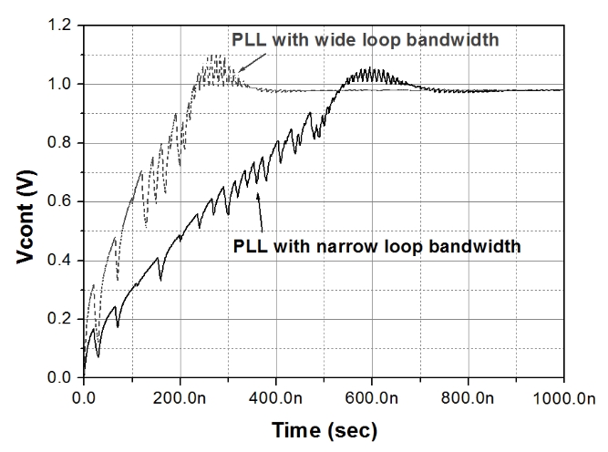
Phase locked loops (PLLs) have been widely used for synchronous clock systems such as microprocessors and communication systems that have a high-speed chip-to-chip interface. In these systems, the PLL must satisfy many design requirements to ensure a high performance. These requirements include phase noise, sideband spur, power consumption, frequency locking range, voltage-controlled oscillator (VCO) gain, and locking time. Furthermore, PLLs for mobile applications should have a small lock time to support the power-saving mode and quick wake-up time. Generally, the lock time of a PLL is controlled by the bandwidth of the loop filter. Fig. 1 shows the waveforms of each control voltage for the VCOs of two PLLs, one with a wide-loop bandwidth of 5 MHz, and another with a narrow-loop bandwidth of 3 MHz. In practice, the waveforms are the results of the behavioral simulation for the analysis of a PLL. The PLL for this simulation has a reference clock frequency of 100 MHz and a divider ratio of 10. The results of the simulation shown in Fig. 1 indicate that the loop bandwidth of a PLL must be increased to reduce the lock time of a PLL. However, this solution deteriorates the performance of the noise filter against the external noise. To minimize the phase jitter of the output clock of a PLL, the bandwidth of the PLL must be narrow.
To solve the issue, [1, 2] have demonstrated a variable-bandwidth scheme in which the loop bandwidth of a PLL is increased to reduce the initial transient time during the PLL locking process. After a PLL approaches the locked state, its loop bandwidth is switched to be narrow to minimize output phase jitter. However, because of its complex architecture, the design and implementation of a stable PLL is not easy.
In this paper, a frequency-to-digital converter (FDC) that measures the frequency of the input reference clock is proposed for a fast-lock PLL. The proposed scheme is based on a conventional charge-pump PLL. The initial control voltage of a VCO is driven toward a reference voltage that is determined by the FDC during wake-up time. Section 2 describes the proposed fast-lock PLL using the FDC. Section 3 examines its implementation and measurement results. In section 4, concluding remarks are presented.
II. PROPOSED FAST-LOCK PLL USING FDC
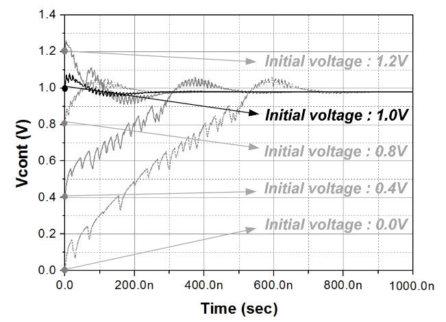
In the general charge-pump PLL with the fixed-loop bandwidth, the lock time of the PLL is determined by the initial control voltage of the VCO. Fig. 2 shows the waveforms of the control voltage for the VCO of the PLL in the case of the initial voltages of 0.0, 0.4, 0.8, 1.0, and 1.2 V. This simulation is achieved in the same environment as that of the behavioral simulator in Fig. 1. The results shown in Fig. 2 indicate that the lock time of the PLL is minimized when the control voltage of the VCO is initialized to the target control voltage for the phase lock.
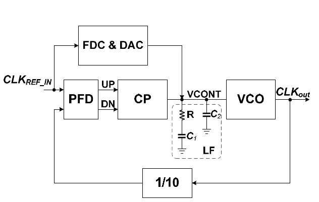
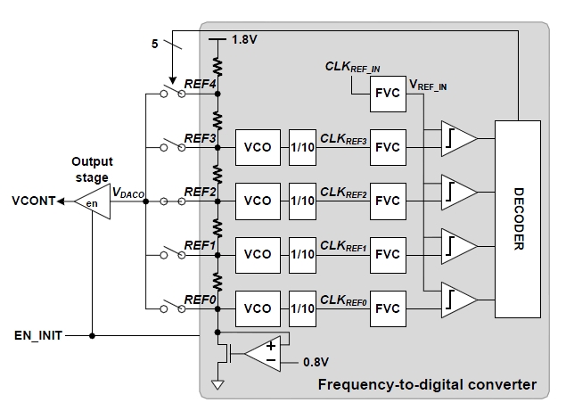
In this work, a PLL is proposed that can set the optimal initial control voltage to achieve the fast-lock time. Fig. 3 illustrates the block diagram of the proposed fast-lock PLL. It consists of the conventional charge-pump PLL and the proposed
The conventional charge-pump PLL consists of a phase-frequency detector (PFD), a charge-pump (CP), a loop filter (LF), a divider, and a VCO. The PFD generates two pulse signals that are proportional to the phase difference between the two inputs. Two pulse signals are driven toward the CP to control the VCO through the LF. In this work, the frequency of the PLL output clock is targeted to be 1 GHz with a 1.8 V supply. This PLL also multiplies the frequency of the reference clock by 10 and generates the four-phase clock.
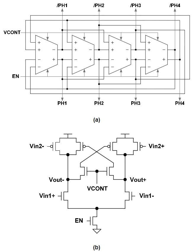
The block diagram of the VCO is shown in Fig. 4a. It has four differential delay cells for a four-phase output clock and its architecture is based on a dual loop for high frequency operation [3]. Fig. 4b shows the circuit of the delay cell. It is based on two inverters that are cross-coupled for differential outputs. As the voltage level of VCONT increases, the strength of the cross-couple of the delay cell increases. Thus, the oscillation frequency of the VCO decreases. To reduce the power consumption in the initial mode for the fast lock scheme proposed in this work, the VCO in the forward path of the PLL is disabled by the control signal, denoted EN in Fig. 4b, until the loop filter is charged with the initial control voltage of the VCO by the
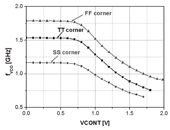
The simulation of the designed VCO was achieved for the three corners, FF, TT, and SS, as shown in Fig. 5. It includes the effect of parasitic capacitance. The simulation condition of the process, voltage, and temperature changes for each corner. The results of the simulation indicate that the designed VCO generates the clock signal with the target frequency, 1 GHz, under the three corners.
The
The input reference clock frequency information (CLKREF_IN) is converted to the analog voltage (VREF_IN) generated by a frequency-to-voltage converter (FVC). The information on each reference voltage is converted to the information on the frequency via the VCO. In this work, a divider ratio of 10 is needed to replicate the feedback path of the PLL. The frequency information divided by 10 is converted to voltage by the FVC to compare its frequency with
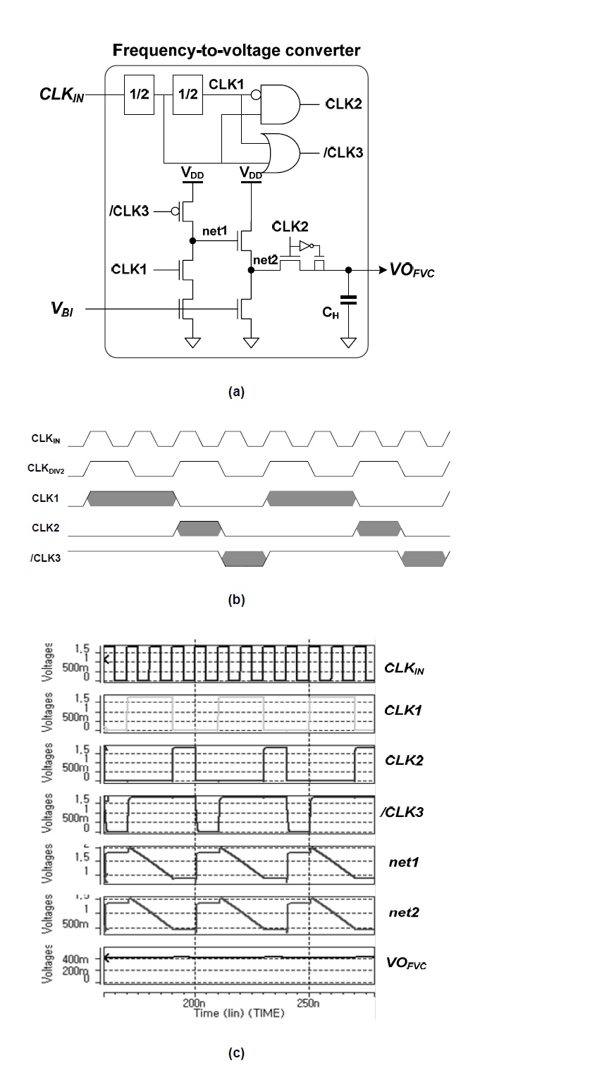
The FVC used in the FDC is designed simply by utilizing a current integrator, as shown in Fig. 7a. Fig. 7b shows the timing diagram of the clock generator to control the FVC. The simulation result of the FVC with a 100 MHz input clock frequency is shown in Fig. 7c. When
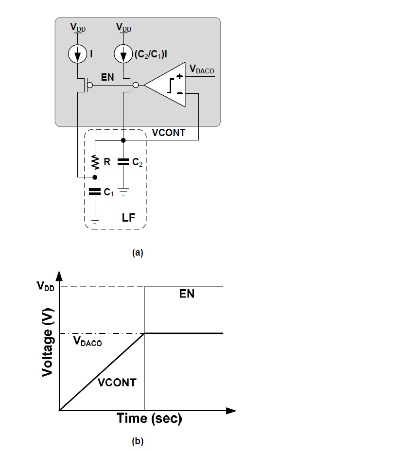
The output stage of the
The simulation of the output stage of the FVC was achieved with the loop filter designed for the PLL, as shown in Fig. 9. According to the simulation results, the slew rate of the output stage designed in this work is 66.7 mV/ns and the worst settling time is about 25.4 ns. The settling time can be reduced by increasing the magnitude of the current sources.
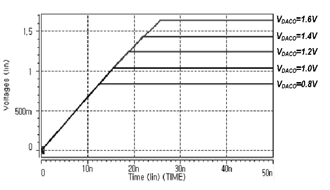
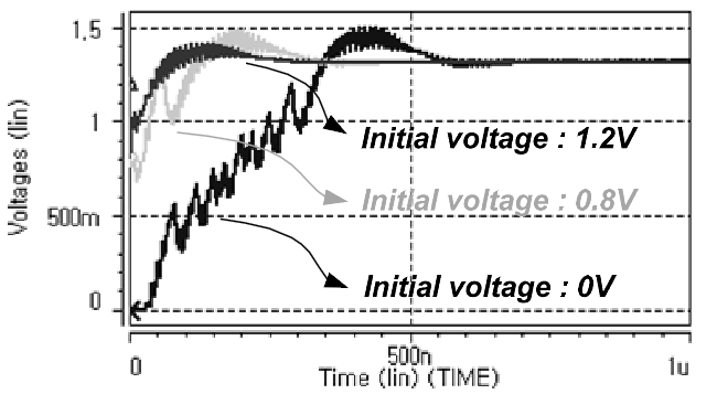
Fig. 10 shows the simulated waveforms of the control voltage for the VCO of the designed PLL in the case of the initial voltages of 0.0, 0.8, and 1.2 V. This simulation is achieved by using HSPICE (Synopsys Inc., Mountain View, CA, USA). The PLL for this simulation has a reference clock frequency of 100 MHz, a divider ratio of 10, and a loop bandwidth of 3 MHz. It is locked when the control voltage of the VCO reaches a voltage of 1.32 V with a supply of 1.8 V.
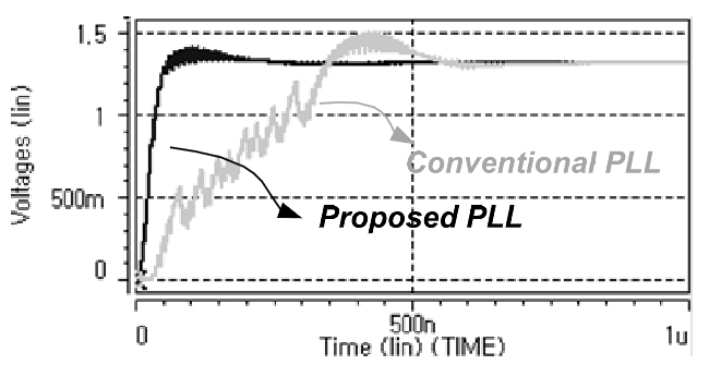
Fig. 11 shows the simulated PLL lock time in the case of the proposed PLL and the conventional PLL. The designed PLL generates a four-phase output clock of 1 GHz and can set the initial control voltage of the VCO controlled by the
Until
III. CHIP IMPLEMENTATION AND RESULT
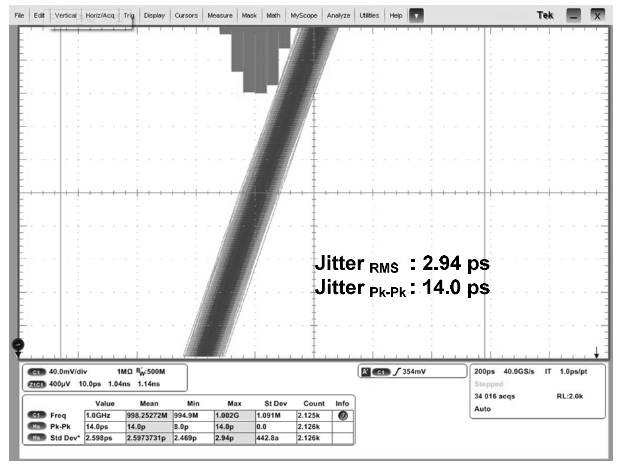
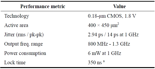
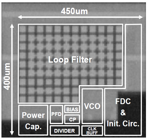
Fig. 12 shows a micrograph of the PLL fabricated in a 0.18-㎛ 1-poly 6-metal complementary metal-oxide semiconductor (CMOS) process with a 1.8 V supply. The active area of the PLL occupies 400 × 450 ㎛2. The power consumption of the PLL with the output clock frequency of 1 GHz is 6 mW. The measured frequency range is from 800 MHz to 1.3 GHz. The root-mean-square (rms) and peak-to-peak jitter are 2.94 ps and 14 ps at 1 GHz, respectively, which are 0.294% and 1.4% of the output clock period, as shown in Fig. 13.
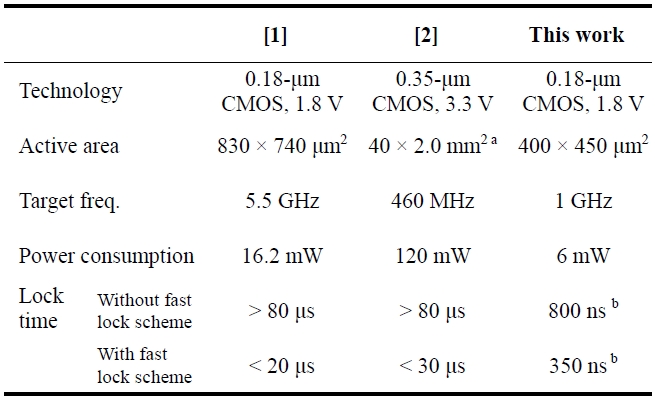
Table 1 is the performance summary of the implemented PLL. Furthermore, Table 2 shows the performance comparison of this work with previous reports. The proposed fast-lock PLL reduces the lock time with a small area and low power consumption.
[Table 1.] Performance summary of fast lock phase-locked loop

Performance summary of fast lock phase-locked loop
[Table 2.] Performance comparison
Performance comparison
A 1 GHz CMOS fast-lock PLL was implemented by using an FDC to measure the frequency of the input reference clock and a DAC to generate the initial control voltage of the VCO. The initial control voltage of the VCO is driven toward a reference voltage that is determined by the frequency of the input reference clock in the initial mode. The proposed PLL was fabricated by using a 0.18-㎛ 1-poly 6-metal CMOS process with a 1.8 V supply. The simulation results show a reduction of up to 40% in the worst-case PLL lock time over the device operating conditions. The rms jitter of the proposed PLL was measured as 2.94 ps at 1 GHz. The area and power consumption of the implemented PLL are 400 × 450 ㎛2 and 6 mW, respectively.