AS the densities of very-large-scale integration (VLSI) circuits and process technologies have been developed quickly in the past several years, performances of embedded processors have been greatly improved and used in many embedded systems including network systems, communication systems, and household appliances. Various technical approaches to performance have been applied during the process implementation of these systems. This is attributed to the development of embedded processors. It is necessary to consider performance improvement and power consumption during a processor design. Although most processors use a delayed branch for normal pipeline operations, pipeline operation delay caused by a delayed branch has become a serious obstacle for improving performance [1-4].
Caches have become the most basic and the most important elements determining the performance of high performance microprocessors with unsatisfyingly limited memory bandwidth provided by the systems. In addition, most of the dynamic power of a processor is dissipated on the clock and data-path related circuits. This is a central part of a low-power design to reduce the dynamic power dissipated on high-activity lines [5, 6].
In this paper, we propose architectures for improving the power and performance of an embedded processor. The architectures are the branch predictor, 4-way set-associative cache architecture for performance improvement and clock-gating logics using observability don’t care (ODC) conditions for a low-power embedded processor [7].
The rest of this paper is organized as follows. Section II briefly reviews the OpenRISC core. In section III, we present the architecture of the 4-way set-associative cache. Section IV shows the dynamic branch prediction algorithm that uses branch target buffer (BTB). Section V presents the clock-gating algorithm using ODC conditions. In section VI, we discuss the performance and the power consumption of the OpenRISC core using the proposed algorithms, followed by the conclusion.
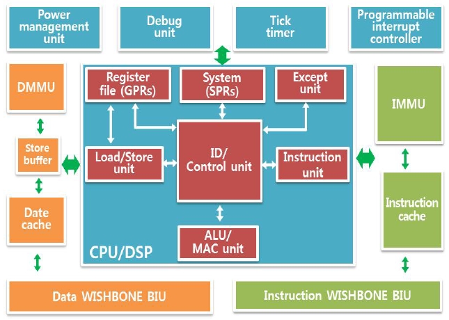
The OpenRISC core is a 32-bit scalar RISC with Harvard micro architecture which has a separated instruction/data bus, 5 stage integer pipeline, and basic digital signal processing (DSP) capabilities. As shown in Fig. 1, the core consists of the CPU, caches, memory management units (MMUs), debug unit, WISHBONE bus interface, and tick timer. The default caches are a 1-way direct-mapped 8 KB data cache and a 1-way direct-mapped 8 KB instruction cache, each with a 16-byte line size. The MMUs are constructed of 64-entry hash-based 1-way direct-mapped translation lookaside buffer (TLB) [8, 9].
III. 4-WAY SET-ASSOCIATIVE CACHE
The disadvantage of the direct-mapped cache used in the old OpenRISC core is a high miss rate when several memory blocks are mapped to one cache block. Therefore, a 4-way set-associative cache is proposed for a low miss rate of the cache. The proposed cache consists of four direct-mapped caches that work in parallel. Data are found in one cache among four by using an address which is stored in one of the four caches.
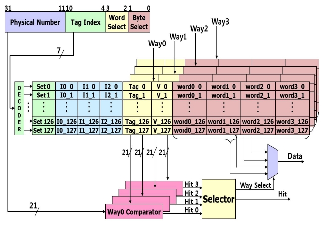
The size of the proposed 4-way set-associative cache is 8 KB. As shown in Fig. 2, it consists of 128 sets, tag comparators, a line decoder, a word multiplexer, and LRU register in which the most recently accessed way is stored.
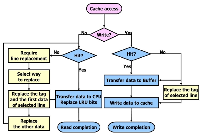
Fig. 3 shows a flow chart of the cache operation when the CPU accesses the memory. If the CPU accesses the memories, the 4-way set-associative cache will be accessed first. If it is a read access from the CPU, the cache will compare the 32-bit physical address with a 21-bit tag, which is one of the four tags stored in 4 tag rams. If a cache hit happens, one of the four words in the hit line of a set will be selected by the word select bit and be transmitted to the CPU. The least recently used (LRU) bit in the accessed line will be updated. If none of the four tags is consistent with the physical address, a cache miss will happen. If a cache miss happens, the entire data of the line will be updated in accordance with the line replacement algorithm.
The proposed 4-way set-associative cache uses the pseudo-LRU algorithm which is one of the line replacement algorithms. The pseudo-LRU algorithm is an algorithm used for implementing the performance of true-LRU with relatively lower cost and area. It is an algorithm that transforms the several ways into one group, used in n-way set-associative cache architectures, and preserves the LRU bits in sets [10, 11].
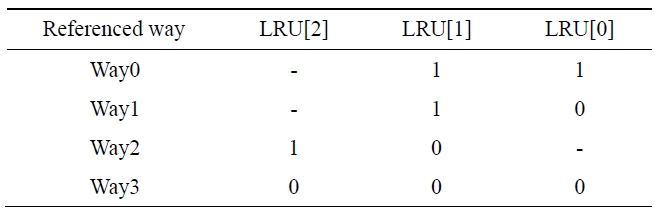
A 4-way set-associative cache consists of 4 sets. To apply the pseudo-LRU algorithm, Way0 and Way1 are transformed into one group and Way2 and Way3 are transformed into another group. There are three bits in the LRU. The two groups are distinguished by the second bit (LRU[1]) of the LRU. The first bit (LRU[0]) distinguishes Way0 and Way1 and the third bit (LRU[2]) distinguishes Way2 and Way3. The 4-way set-associative cache algorithm updating the LRU bits is shown in Table 1. If the referenced current way is Way0 or Way1, LRU[1] will be set to 1. If the way is Way2 or Way3, LRU[1] will be set to 0. In the case that Way 2 or Way3 is referenced, LRU[2] is set to 1 or 0. The symbol ‘-’ means the value before the update is kept.
[Table 1.] Algorithm of pseudo-least recently used (LRU) policy

Algorithm of pseudo-least recently used (LRU) policy
IV. DYNAMIC BRANCH PREDICTION WITH BTB
To alleviate the disadvantage of a delayed branch, which inserts unnecessary instructions, we propose a dynamic branch prediction algorithm using BTB. BTB is a cache memory related to the instruction fetch (IF) pipeline stage and stores the executed branch prediction address and the branch target address [12-15].
At the IF pipeline stage, the BTB compares the fetched address with the previously branched instruction stored in the BTB. If the addresses are the same, it will predict whether a branch happens or not. If the prediction shows that a branch happens, the branch target address will be used as the next program counter (PC) value and the instruction in the branch target address will be fetched. The branch target address instruction is decoded at the instruction decode (ID) stage when a branch happens. Therefore, a branch is executed without a pipeline delay.
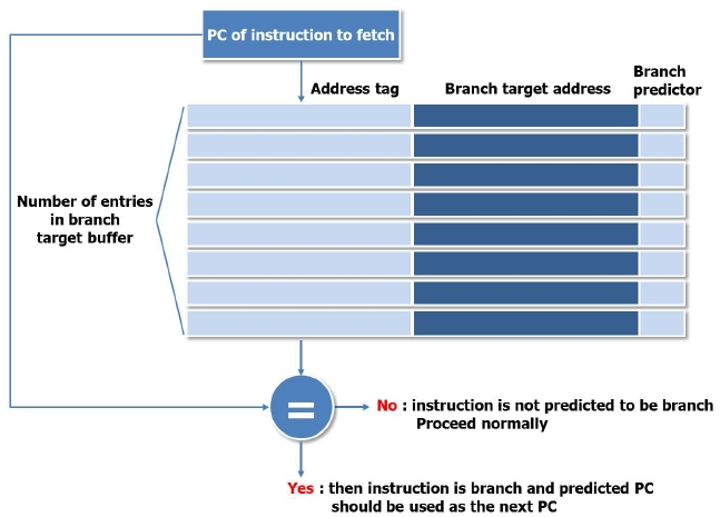
Fig. 4 shows the BTB architecture applied to the OpenRISC core. The BTB consists of address tag memory, branch target address memory, and a tag comparator.
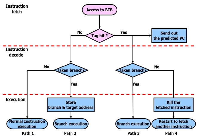
Fig. 5 shows the BTB operation flow chart. The CPU transmits a PC value to the instruction cache and the BTB for the instruction fetch.
However, if the branch does not take place, the instruction of the fetched branch target address will be flushed and a new instruction will be fetched. In this case, at the IF stage, if the PC tag field is not coincident with the selected line address tag, it will be checked to decide whether to branch or not at the ID stage. If the branch takes place, the BTB will update the selected line address tag and branch target address. If it does not take place, the decoded instruction will be executed. Table 2 shows the branch penalties to the paths of Fig. 5.
[Table 2.] Branch penalties of the branch target buffer path
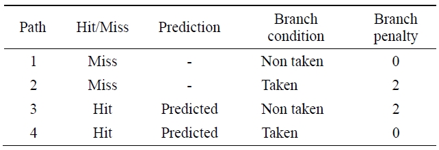
Branch penalties of the branch target buffer path
The penalty of the path 1 is 0, because a branch is not taken. The penalty of path 2 and 3 is 2 since the instruction of the branch target address is fetched when a branch is taken. The penalty of path 4 is 0 because the instruction of the branch target address is fetched before a branch is taken.
V. CLOCK-GATING ALGORITHM WITH ODC OPERATION
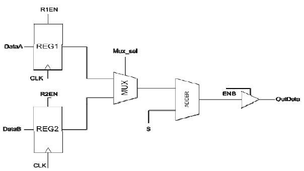
Generally, on a sequence circuit, input data is inserted into a register on the active clock transition. When the output of the register is transmitted to the final output through combinational circuits, it sometimes becomes meaningless. In this case, the output of the register is a don’t-care condition. Fig. 6 shows a data path circuit example. When the control signal En_B equals 0, whatever the input data of the tri-state buffer is, the value of OutData is a high impedance value. This means the input data to the tri-state buffer, signal DataA and signal DataB, is meaningless to the Adder operation. Thus, it is unnecessary to insert the clock to REG1 and REG2 when the value of ENB is 0 [6, 16].
The select signal (Mux_sel) of the multiplexer selects one of the input data from DataA or DataB. When the input data of DataA is selected, which means the value of the select signal is 0, DataB is in the don’t-care condition. If the select signal is 1, DataA will be in the don’t-care condition. It is unnecessary to insert the clock to the register that is in the don’t-care condition. The clock-gating algorithm using the ODC operation is designing clock-gating logic by operating the don’t-care condition as stated above. This algorithm reduces power consumption by preventing transitions of input data and the logic connected to the input data by the gating clock.
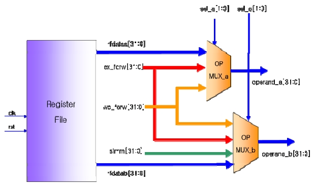
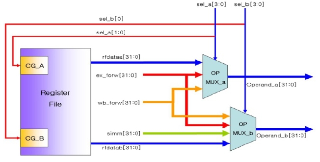
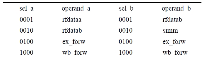
The ODC operation is applied to the operand multiplexer to reduce the power consumption of the OpenRISC core. The operand multiplexer receives the two operands and transfers them to the modules such as the arithmetic logic units (ALU) and load-store unit (LSU). Fig. 7 shows the block diagram of the operand multiplexer and register file. The operand multiplexer selects one of the data points among the forwarding data (ex_forw) in the execution stage, forwarding data (wb_forw) in the write back stage, immediate data (simm) and the data (rfdataa, rfdatab) transferred to the register file, and transfers it to operand a and operand b.
In order to apply the ODC operation, the operand multiplexer was modified into a one-hot multiplexer. A one-hot multiplexer is a data select circuit that has a number of select bits that equals the number of input signals. If one of the select bits is activated, the output will be the input data corresponding to the select bit. The 2-bit select signals, sel_a and sel_b, of the one-hot multiplexer turn out to be 4-bit signals.
Table 3 shows the select signals and the input signals of the modified multiplexers. When the value of the select signal sel_a is 0001 or 0010, rfdataa is selected and when the value of the select signal sel_b is 0001, rfdatab is selected. Thus, as shown in Eq. 3 and Eq. 4, the signal rfdataa of the register file is in the ODC condition when the first or the second bit of the signal sel_a is 0 and the signal rfdatab of the register file is in the ODC condition when the first bit of the signal sel_b is 0.
[Table 3.] Operands for select signals of one-hot multiplexers
Operands for select signals of one-hot multiplexers
Fig. 8 shows the logic circuit of the operand multiplexer and the register file added to the clock-gating logic using the ODC operation condition.
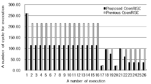
In order to compare the performance of the proposed OpenRISC architecture with the previous one, the inverse transform (IT) and inverse quantization (IQ) blocks of the H.264 decoder were used as test programs. The IT and the IQ are executed 26 times per 16 × 16 macroblock in the H.264 decoder. Fig. 9 shows the number of execution cycles for the IT after the IQ with the previous OpenRISC core, OpenRISC1200, and the proposed OpenRISC core. The cycle numbers of the first IT after the first IQ are both 260, but the cycle number of the proposed architecture goes down to 115 and the cycle number with the previous architecture goes down to 206 as the process goes on. After the 18th IQ, the cycle number of the Hadamard IT with the previous architecture is 97, but the cycle number of the proposed architecture including the 4-way set-associative cache goes down from 97 to 37. Therefore, the performance is improved by 46%. When the core executes the 17th IT, the instruction for the IT remain in the cache because the 17th IT executes after the 16th IT. Therefore, the number of cycle in the 17th execution is reduced rapidly. For the same reason, the number of cycle in the 20th execution is reduced rapidly.
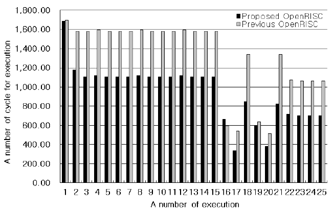
Fig. 10 shows the cycle number of the IT before the IQ starts. After the IT, the repetitive execution cycle numbers of the IQ with the previous core and the proposed core are 1,581 and 1,108 respectively. The cycle numbers of the Hadamard IT are 1,061 and 701, respectively. Therefore, the performance is improved by 29%. When the core executes the 17th IQ, the instruction for the IQ remains in the cache because the 17th IQ executes after 16th IQ. Therefore, the number of cycle in the 17th execution is reduced rapidly. For the same reason, the number of cycle in the 20th execution is reduced rapidly.
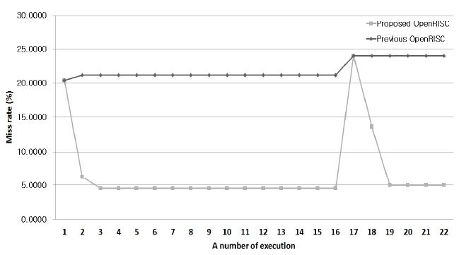
Fig. 11 shows the miss ratios of the previous core and the proposed core. In the first execution, the miss ratios are both 20.37% in the previous and the proposed design. As the execution time goes on, the miss ratio of the proposed design decreases to 4.5%, but the miss ratio of the previous design increases to 21.15%.
The miss ratios of the Hadamard IT execution are both 24% in the two cores. As the time goes on, the miss ratio of the proposed architecture decreases to 5%, but the miss ratio of the previous core increases to 24%. Thus, the miss ratio of the proposed architecture decreases by 15% compared to the previous one.
For the purpose of comparing dynamic power consumption, the Design Compiler and Power Compiler of Synopsys Corp. were used with the Chartered 0.18 cell library.
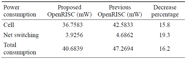
As shown in Table 4, the power consumption of the proposed OpenRISC core, which considered dynamic power consumption and applied clock-gating using ODC operation, is decreased by 16.2% compared to the previous one.
[Table 4.] Comparison of power consumption

Comparison of power consumption
For the purpose of performance improvement and improving power consumption of an embedded RISC core, the 4-way set-associative cache architecture, a branch prediction algorithm using a BTB, and clock-gating logic applied to the ODC operation are proposed.
The 4-way set-associative cache, the block of which maps to four blocks of a memory, is used to decrease the high miss ratio of the OpenRISC core cache. The branch prediction using a BTB, which stores the branch address and the target address, decreases the number of cycles of delay. The clock-gating using ODC operation carries out the don’t-care conditions of the inputs to gate the clock of the registers to reduce the dynamic power consumption of the OpenRISC core.
As a result, the performance of the proposed core is improved by 29% and the dynamic power is reduced by 16% compared to the previous one. Therefore, the performance and the power consumption of the proposed core are both improved.