A 40-MS/sec 10-bit pipelined analog to digital converter (ADC) with a 1.2 Vpp differential input signal is proposed. The implemented pipelined ADC consists of eight stages of 1.5 bit/stage, one stage of 2 bit/stage, a digital error correction block, band-gap reference circuit & reference driver, and clock generator. The 1.5 bit/stage consists of a sub-ADC, digital to analog (DAC), and gain stage, and the 2.0 bit/stage consists of only a 2-bit sub-ADC. A bootstrapped switch with a constant resistance is proposed to improve the linearity of the input switch. It reduces the maximum VGS variation of the conventional bootstrapped switch by 67%. The proposed bootstrapped switch is used in the first 1.5 bit/stage instead of a sample-hold amplifier (SHA). This results in the reduction of the hardware and power consumption. It also increases the input bandwidth and dynamic performance. A reference voltage for the ADC is driven by using an on-chip reference driver without an external reference. A digital error correction with a redundancy is also used to compensate for analog noise such as an input offset voltage of a comparator and a gain error of a gain stage. The proposed pipelined ADC is implemented by using a 0.18-μm 1-poly 5-metal CMOS process with a 1.8 V supply. The total area including a power decoupling capacitor and the power consumption are 0.95 mm2 and 51.5 mW, respectively. The signal-to-noise and distortion ratio (SNDR) is 56.15 dB at the Nyquist frequency, resulting in an effective number of bits (ENOB) of 9.03 bits.
Over the past few decades, the designs for many pipelined analog-to-digital converters (ADCs) have been published for use in communication systems and image signal processing systems [1-3]. Recently, low power consumption and small area have become two of the most significant requirements for mobile systems. The pipelined ADCs in the literature [3] and [4] have reduced the power consumption and chip area by eliminating a sample-and-hold amplifier (SHA). To implement the pipelined ADC without an SHA, the design of the input sampling circuit is important to enhance the dynamic performance of an entire ADC. Specifically, the switching clock between the multiplying digital-to-analog converter (MDAC) and the ADC in the first stage should be synchronized to produce an accurate sample of the input analog signal. Thus, an identical bootstrapped switch was used for the clock phases of both the MDAC and ADC [3].
In this work, a 1.8 V 40-MS/sec 10-bit pipelined ADC without an SHA is proposed to reduce hardware and power consumption. It uses a bootstrapped switch with a constant resistance to improve the linearity of the input sampling circuit [5]. Furthermore, it includes the on-chip reference driver, which generates the bias voltage of the entire analog block including the reference voltage for an ADC of each stage. Section II describes the architecture and circuits of the proposed pipelined ADC. Section III examines its implementation and performance. In section IV, concluding remarks are presented.
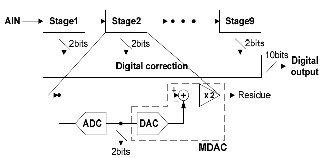
The proposed pipelined ADC consists of the analog block of nine stages and the digital block, which corrects the error noise generated in the analog block, as shown in Fig. 1. Each stage consists of an ADC, a DAC, and an amplifier with the voltage gain of two. However, the last stage includes only a 2-bit ADC.
Each stage resolves two bits with an ADC, subtracts this value from its input, and amplifies the resulting residue by a gain of two while it samples and holds the output of the previous stage. The stages are buffered by switched-capacitor gain blocks that provide a sample-and-hold between each stage, allowing concurrent processing. Each stage outputs the 2-bit digital code, and the 18-bit digital code from nine stages is supplied to the digital correction block. Then, the 10-bit binary digital code is finally generated by the digital correction block. Because the 18-bit digital code is sequentially generated for the sampled input analog signal, the digital correction block has a register composed of a D flip-flop to store the digital code supplied from each stage.
The analog block composed of nine stages generates the 18-bit digital code including the redundancy bits to correct for analog noise errors such as the offset voltage of a comparator and operational amplifier and the variation in the reference voltage. Thus, the pipelined ADC can increase the accuracy by compensating for the analog noise through digital error correction. This architecture with digital correction relaxes the constraints on the comparator offset voltage and direct current (DC) operational amplifier gain. Even if each stage generates the 2-bit digital code, this code effectively has the information of 1.5 bits. Actually each stage except the last one has three comparators for an ADC that has thresholds at +VREF/4 and -VREF/4 [1]. The input signal ranges from -VREF to +VREF (differential). The designed pipelined ADC has a differential input range of 1.2 Vpp with a 1.8 V supply. The voltage levels of -VREF and +VREF are 0.6 V and 1.2 V, respectively.
The proposed pipelined ADC uses the first 1.5 bit/stage including a bootstrapped switch with a constant resistance instead of a SHA. It results in the reduction of the hardware and power consumption. It also increases the input bandwidth and dynamic performance.
>
B. Input Sampling Circuit of First Stage
A SHA samples and holds the consistently transitional analog signal by using two periods of sample and hold. This results in the improvement of the dynamic performance in an ADC. Usually, an SHA consists of a holding capacitor, a sample switch, and an operational amplifier. Thus, this increases the power consumption and chip area, and limits the input bandwidth.
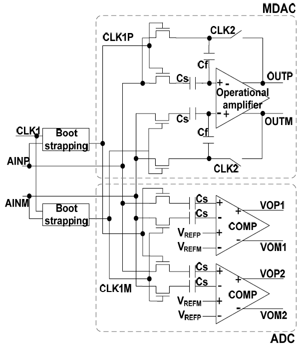
In this work, an SHA is removed to have the wide input bandwidth over the Nyquist frequency and to reduce the power consumption and chip area. Fig. 2 shows the input sampling circuit of the first stage.
The input sampling circuit of the proposed pipelined ADC is implemented by synchronizing the clock phase between an ADC and an MDAC instead of using an SHA. While an MDAC and an ADC sample the analog input signal, the resistive and capacitive time constant of each path, which is determined by the product of the turn-on resistance of each analog switch and the load capacitance, should be maintained as constant. Thus, the identical bootstrapped switch is used for the clock phases of both the MDAC and ADC only in the first stage. This improves the dynamic performance by having a constant resistance even if the analog voltage level changes. Furthermore, the sampling capacitors (CS) of the MDAC and ADC have an identical value and are implemented by using a metal-insulator-metal (MIM) capacitor.
>
C. Bootstrapped Switch with Constant Resistance
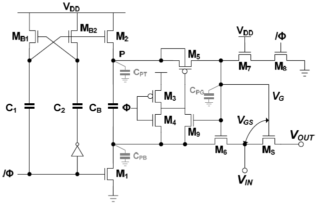
In most highly accurate ADCs, a bootstrapped analog switch is used for sampling in sample-hold circuits. It provides constant on-resistance by maintaining the gate-source voltage (VGS) of the sampling switches independent of the input signals. This results in the improvement of the precision and linearity of the sample-hold circuits. Fig. 3 shows the circuit diagram of the conventional bootstrapped switch using the capacitor (CB) [1].
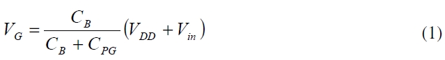
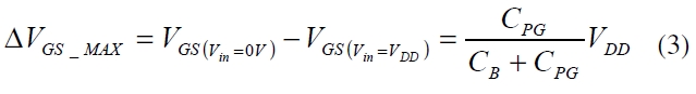
MS operates as the sampling switch, turning on during phase Φ and off during /Φ. When Φ is low, VDD is applied across CB by turning M1 and M2 on. M6 and MS simultaneously turn off as the node voltage VG is switched to ground. When Φ is high, the bottom plate of CB is connected to VIN, and the top plate of CB and the VG node are shifted to the voltage level of VDD + VIN as M5 and M6 turn on. Thus the VGS of MS is ideally determined by VDD, which is independent of VIN. However, this approach may lead to variations in VGS due to the change of VIN when the parasitic capacitors (CPT, CPB, and CPG) shown in Fig. 1 cannot be ignored. Actually, CPG may have a relatively large capacitance value due to the gate of the analog switch and route path while the capacitance values of CPT and CPB are small. The voltage levels of VG and VGS are determined by the charge sharing between CB and CPG, as shown in Eq. (1) and (2). Thus the maximum variation of VGS when VIN changes from ground to VDD is expressed as Eq. (3).
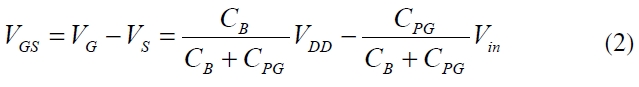
As a result, the node voltage VG is not determined by VDD + VIN, and the VGS of MS is dependent on the input signal due to CPG.
In the pipelined ADCs, the input-sampling switch (MS) usually uses a large transistor to reduce the on-resistance of the input switch. This results in the increase of the capacitive load (CPG) at the VG node of the input-sampling switch. Thus, the value of VGS has the variation of several tens of mV even if a bootstrapped switch is used.
A bootstrapped switch is used only for the differential analog input signal. Also, the pipelined ADC uses a multi-input-sampling switch instead of one separate sample-hold circuit, as shown in Fig. 2. When the gate voltage of a bootstrapped switch is shared as part of the multi-input-sampling switch, the capacitive load of the gate node of the bootstrapped switch increases.
Thus a gate node of a sampling transistor is not constantly boosted by amount of VDD from the analog input signal, VIN. Furthermore, the input-sampling switch (MS) usually uses a large sized transistor to reduce the on-resistance of the input switch. This results in the increase of the capacitive load (CPG) at the VG node of the input-sampling switch. Thus, the value of VGS has the variation of several tens of mV even if a bootstrapped switch is used.
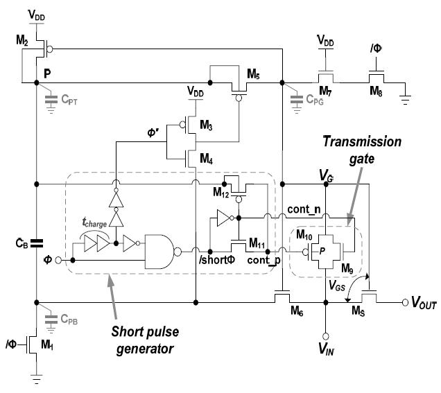
The bootstrapped switch with a constant on-resistance is proposed in this work. To implement this bootstrapped switch, the initialization circuit of the bootstrapped switch is added into the conventional bootstrapped switch, as shown in Fig. 4. The added initialization circuit is composed of a transmission gate and a short pulse generator.
The transmission gate is inserted between the VG and VIN nodes of Fig. 4 and is controlled by the short pulse generator. Also, the Φ’ signal generated in the short pulse generator is supplied for the gate node of M3 and M4 in Fig. 4. When Φ goes high (/Φ goes low), the voltage of the P node changes from VDD to VDD+VIN. Simultaneously, the VG node is charged from ground to VIN by the inserted transmission gate during a short period (tcharge). At this time, the P and VG nodes are separated by turning M5 off because the gate signal of M3 and M4 is delayed from the Φ signal. After the VG node is charged to the voltage level of VIN, the charge sharing between the P and VG nodes is achieved as M5 is turned on. The effect of CPG is minimized by the above mentioned process. Thus the variation of VGS (ΔVGS) is reduced as the voltage level of VIN changes. The short pulse generator supplies the control signals for the transmission gate (cont_n, cont_p) and the gate of M3 and M4 (Φ’).
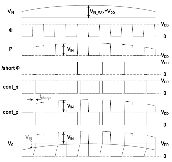
When Φ goes high, the cont_n and cont_p signals have the voltages of VDD and ground, respectively, to turn the transmission gate on during the short period of tcharge, which is the time in which the VG node reaches the voltage level of VIN. Except the initial charging period for the VG node, the cont_p signal follows the voltage of the P node to turn the PMOS transistor of the transmission gate off. Also, it is required to connect the bulk node of M10 to the P node because the voltage level of the VG node can be changed from ground to VDD+VIN. Fig. 5 shows the timing diagram of the bootstrapped switch shown in Fig. 4.
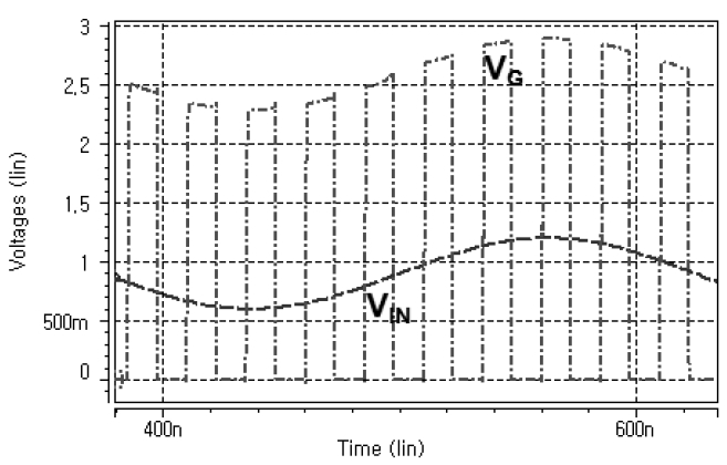
Fig. 6 shows the simulation results of the bootstrapped switch. The frequency of the input signal (VIN) and clock (Φ) are 4 MHz and 40 MHz, respectively. The VG node can confirm VDD+VIN with a 1.8 V supply.
III. CHIP IMPLEMENTATION AND RESULT
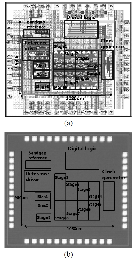
The proposed 40-MS/sec 10-bit pipelined ADC was implemented by using a 0.18-um 1-poly 5-metal CMOS process with a 1.8 V supply. Fig. 7a and 7b show the layout of the designed pipelined ADC and the microphotograph of the implemented pipelined ADC.
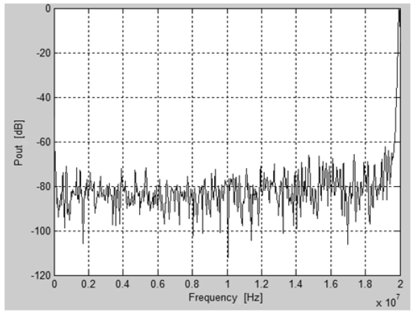
The chip area, including the power decoupling capacitor, and power consumption were 0.95 mm2 and 51.5 mW with a supply voltage of 1.8 V, respectively. Fig. 8 shows the fast fourier transform (FFT) result of the pipelined ADC. The SNDR of the pipelined ADC was 56.15 dB at the Nyquist frequency, resulting in an ENOB of 9.03 bits. Table 1 is performance summary of the proposed pipelined ADC.
[Table 1.] Performance summary of designed pipelined analog to digital converter
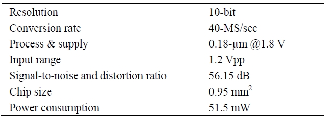
Performance summary of designed pipelined analog to digital converter
A 40-MS/sec 10-bit pipelined ADC with 1.2 Vpp input range was implemented by using a 0.18-μm CMOS process with a 1.8 V supply. The implemented pipelined ADC consisted of an ADC, DAC, gain stage, and digital block. The proposed pipelined ADC increased the linearity by using the bootstrapped switch. The pipelined ADC using an on-chip reference driver instead of an external reference voltage was designed. The pipelined ADC has the SNDR of 56.15 dB and ENOB of 9.03 bits at the Nyquist frequency. The chip area including the power decoupling capacitor and power consumption are 0.95 mm2 and 51.5 mW, respectively.