Graphene has attracted the attention of the device community because it has several excellent electrical properties, such as high current drivability [1-4], high mobility [5], and low noise characteristics [6-8], that are useful in device applications. However, the zero bandgap of graphene limits applications that need a high on-off ratio and rectification [9]. Several methods that have been investigated to create a bandgap, such as a bilayer stack of graphene [10,11], doping [12], and nano ribbon structure [13] are known to compromise mobility; i.e., graphene with a larger bandgap tends to have lower mobility, diluting its benefits [14].
There are several challenges deterring the stabilization of graphene device properties, such as hysteresis [15,16], high electrical contact resistance [17-19], and poor substrate adhesion. These properties have been studied extensively, but only limited progress has been made so far. One of the reasons behind this slow progress might be the inaccurate assessment of device characteristics, especially errors due to hysteretic behaviors. Yet, a systematic approach to review the validity and efficacy of test methods used for graphene devices has been very limited. For example, qualitative studies of hysteresis have not been very useful in the reduction of hysteresis because it is difficult to identify any specific physical mechanism responsible when the hysteresis is measured with a wide range of biases over a time scale much longer than typical charge trapping times.
In this paper, major obstacles in the electrical characterization of graphene devices will be discussed and countermeasures to improve electrical characterization methods will be presented.
2. Silicon Devices Versus Graphene Devices
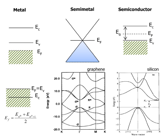
The most significant difference between silicon and graphene devices in terms of device physics is the band structure, as shown in Fig. 1. The location of the Fermi level, EF, in sili-
con indicates the concentration of majority and minority carriers in the bulk. Graphene is often called a “semimetal” because of its zero bandgap, but its carrier concentration can be modulated by an external bias. When the EF is at the cross point of two cones, as shown in Fig. 1, the carrier density is zero (ideally) because there are no available states. As EF moves up (or down) due to an external positive (or negative) bias like other metals, carriers with a density of n = C (V-VDirac) /q are induced. When the EF is within the upper side of the cone, electrons are populated, whereas when the EF is located within the lower cone, holes are induced. In graphene, the location of EF defines only the majority carrier concentration; the minority carriers can be ignored because their lifetime is extremely short.
In silicon, when the EF is modulated by an external bias, there is a certain delay to establish the thermal equilibrium carrier distribution, because thermal generation of minority carriers usually occurs on the order of μsec, unless the minority carriers are supplied from a carrier reservoir such as a highly doped junction or metal contacts. In graphene, the carrier supply concept is vague because electrons and holes behave like a massless Dirac Fermion and the direction of the k vector determines whether the carriers are holes or electrons. The electron and hole population in graphene does not need an external carrier supply, but an external potential change to modulate the position of EF is enough to populate carriers in the graphene. Carriers can be supplied from external contacts, but the physics of external carrier supply through a metal contact has not been clearly understood, because the band alignment at metal and graphene contact is still in the early stage of research.
Carriers in n-type and p-type graphene regions can be tunneled into other regions with zero or minimal scattering through a Klein tunneling mechanism [20]. Thus, there is no rectification at the pn junction of graphene. This is a very significant limitation for the graphene device because rectification was the basic function of electronic applications since early 1900s. In fact, without rectification, the electrical function of graphene that
is useful for electronic application is limited to a conductivity modulation up to ten times only.
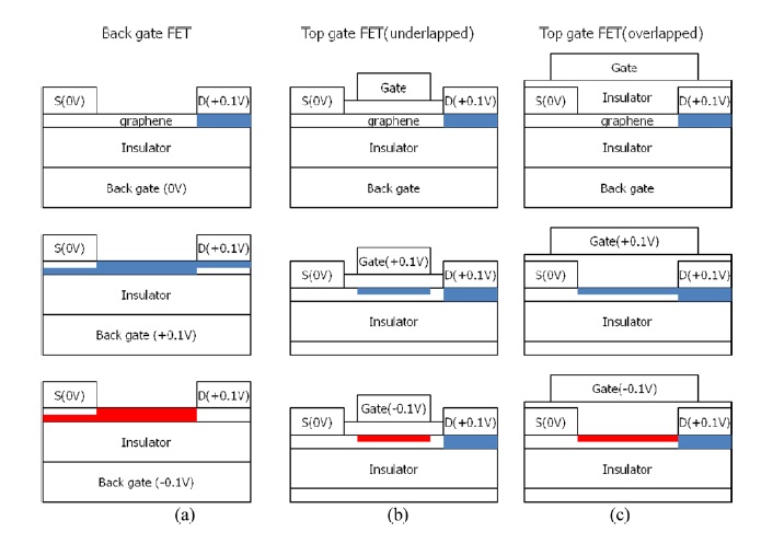
Fig. 2 shows typical graphene device structures with front and back gate under various bias conditions. The metal contact to graphene works as a heat sink or source but, according to the recent study of Ravi et al., it does not change the Fermi level of the graphene. In this case, the gate potential coupled to the graphene channel through the insulator will primarily determine its carrier types and concentrations. Capacitive gate coupling of graphene devices is different from that of silicon devices because the graphene channel does not have a surface potential or band bending in a vertical direction due to its monolayer structure. Instead a quantum capacitance in Cg -1=Cox -1+Cq -1 determines the gate coupling to the graphene channel. Here, Cg is the gate capacitance and Cox is the insulator capacitance. Cq is the quantum capacitance that represents the capacitive response of carriers in the graphene channel, which is closely related to the E-k diagram and density of states [21,22].
As mentioned above, different carrier types in the channel do not hinder the movement of carriers in graphene because electron and holes can tunnel through other regions rather freely through Klein tunneling [20]. However, a low carrier concentration region between the gate and source/drain at an underlapped top gate structure shown in Fig. 2b increases the series resistance and device scattering. At the overlapped gate structure shown in Fig. 2c, a pnp type channel can be induced. Since a realistic system does not have ideal Klein tunneling, finite scattering can still occur at the pnp structure and degrade carrier transport performance. Unfortunately, carrier scattering at carrier puddles, junctions, adsorbed charges or other factors are mixed and it is difficult to distinguish the differences. Thus, the interpretation of current-voltage (I-V) characteristics in graphene devices is quite complex. When there is non-uniform scattering in a sili-
con channel, there are several test methods to monitor the interface problems using a bulk current, such as the charge pumping method or DC I-V method. Unfortunately, in a graphene device, channel probing is not easy because of the monolayer structure. Note that this behavior will become more complex when a small bandgap is generated in the graphene.
4. Hysteretic Device Characteristics
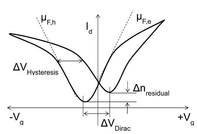
I-V curves of graphene devices represent the conductance modulation due to carrier density modulation in the graphene. As mentioned several times, there are many factors affecting the carrier concentration. Hysteretic I-V curves shown in Fig. 3 summarize another aspect of challenges in the interpretation of I-V curves.
Often, the origin of hysteresis has been interpreted as a result of charge trapping at a graphene-substrate interface or underlying dielectric [23-25]. However, several papers on hysteresis have reported time constants ranging from μsec to a few hundred seconds [14,26,27], indicating that many different physical mechanisms in addition to charge trapping are associated with the hysteretic I-V curves. The I-V curve shown in Fig. 3 assumes that the left branch is an intrinsic I-V curve free from the influence of charge traps surrounding the graphene. The shift in a minimum point of the right I-V curve after a positive bias sweep is due to the difference in the residual charges in the graphene that are generated during the bias sweep in the electron branch and the hole branch respectively. In the case of a silicon MOSFET with high-k dielectric, the charge trapping in a high-k dielectric was primarily due to a positive bias, and a low level of negative bias could be used to detrap the charge to get an intrinsic I-V curve. Unfortunately, in a real graphene device, it is not possible to define an intrinsic branch of I-V curves because even a negative bias sweep can also generate hole trapping. As a result, mobility values extracted from the slope of the drain currentgate voltage (Id-Vg) curves cannot represent the intrinsic field effect mobility of graphene. This situation seems to be similar to the case of a poor quality SiO2 used in the 70's, or high-k dielectrics with charge trapping, resulting in the underestimation of mobility in silicon devices.
Depending on the origin of the hysteresis, different test methods can be used to reduce the errors from the hysteretic I-V curves of silicon devices. If the quality of SiO2 is poor, positive mobile charges can be pushed away from the interface by applying a negative gate bias at an elevated temperature, allowing pseudo-intrinsic device properties to be studied. In high-k dielectric development, fast pulse I-V could be used to minimize the influence of the charge trapping in a high-k dielectric because the charge trapping took on the order of μsec. If the test can be completed before the charge can accumulate within a high-k dielectric, an intrinsic I-V curve can be obtained [28,29]. There is no clear understanding on how an intrinsic I-V curve can be obtained from hysteretic I-V curves of graphene.
On the other hand, graphene seems to have many different charging sources, including some defects exhibiting fast trapping behaviors. With a limited understanding of the sources causing hysteresis, it is not easy to find a test method to measure intrinsic properties. Thus, conventional I-V measurements used for graphene devices showing hysteretic behaviors inherently include very significant errors [14].
5. Analysis of Current Voltage Characteristics
In silicon devices, Id-Vg curves need several corrections before they are used as an indicator of device performance. For example, all of the parameters used in Eq. (1), W, L, Cox, VT, and Vd, should be well defined to extract an effective mobility. An accurate surface potential and total number of minority charges accumulated with the channel are also needed, since Vd, L and VT are not well defined for short channel devices, and there are many correction methodologies reported in the literature.
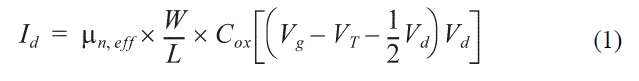
First, the Id reduction due to effective Vd reduction by series resistance components should be recovered [30]. Several methods to normalize the drain current to Id at Vd from Vd’ = Vd-IdRs have been developed and are readily available in text books. Second, an effective channel length, Leff, should be determined for short channel devices. Several methods to extract Leff have been developed for different channel length regions in silicon devices because Leff is strongly affected by extension doping and halo doping conditions [31]. Determination of VT is also a complex procedure because there is no clear definition of threshold voltage that can be used to physically define VT.
For graphene devices, none of the above methods are relevant because there is no doping and junction formation. The effect of series resistance is manifested by a current saturation, shown by the separation of the I-V curves from the dashed linear lines in Fig. 3. However, series resistance is not a pseudo constant as in a silicon device, but it can be strongly affected by a device structure and a gate bias, which modulates the carrier concentration of metals-graphene contact, as illustrated in Fig. 2 [32]. In the case of silicon, the effect of series resistance can be ignored when the current level is low, i.e. for long channel devices. In a graphene device, the current level is very high even at moderate Vd because of low resistance at the channel. Thus, it is not easy to ignore the effect of series resistance.
In a graphene device, both W and L are not well defined, even in large size devices. The carrier concentration of graphene is heavily affected by many environmental factors and carriers within a graphene channel form a non-uniform puddle-like concentration distribution [33]. This means the effective channel length and width cannot be defined clearly. As a result, the current scattering is very severe even when channels are patterned with a well-established lithography process. This problem gets worse when the channel narrows down to nano ribbon size due to the influence of edge states.
In addition to the problem of W and L, minimum current point, VDirac which is analogous to Vth in a silicon MOSFET is also strongly affected by surrounding charges as discussed above. When there is a hysteresis in I-V curves, none of two VDirac points are free from residual charges. Ambiguity in the Dirac point results in the ambiguity in the carrier concentration, which is critically important in the definition of mobility in the graphene FET. Lastly, Cox is also a problem in a graphene device because capacitive coupling in graphene devices depends strongly on the bias and does not saturate as in silicon devices. Additionally, the dispersion of capacitance has not been studied in detail. With silicon devices, the capacitive component of the interfacial state, Cit, is included in the gate capacitance model, but a model to include the effect of charge exchange between graphene and its environment has not been developed yet.
Another factor implicitly used in Eq. (1) is temperature. In Eq. (1), the temperature of the device is fixed, but considering the case of ultrathin silicon-on-insulator (SOI) devices, it is clear that the temperature of graphene devices will change during device operation due to the self-heating effect [34]. In general, a very low drain bias or short operation time should be used to avoid temperature-induced device degradation, but no such effort has been reported for a graphene device.
Theoretically, Eq. (1) can be used for graphene devices because of its narrow surface channel operation, but parameters in the equation still have too many uncertainties. Nevertheless, some parameters should be defined to compare the devices and field effect mobility derived from Eq. (1) [9]. Then, what can be done to extract device parameters that are useful to some degree?
Major unknowns should be eliminated before extracting device parameters from I-V characteristics. If this is not possible, a new test approach with minimal influence from environmental factors should be considered.
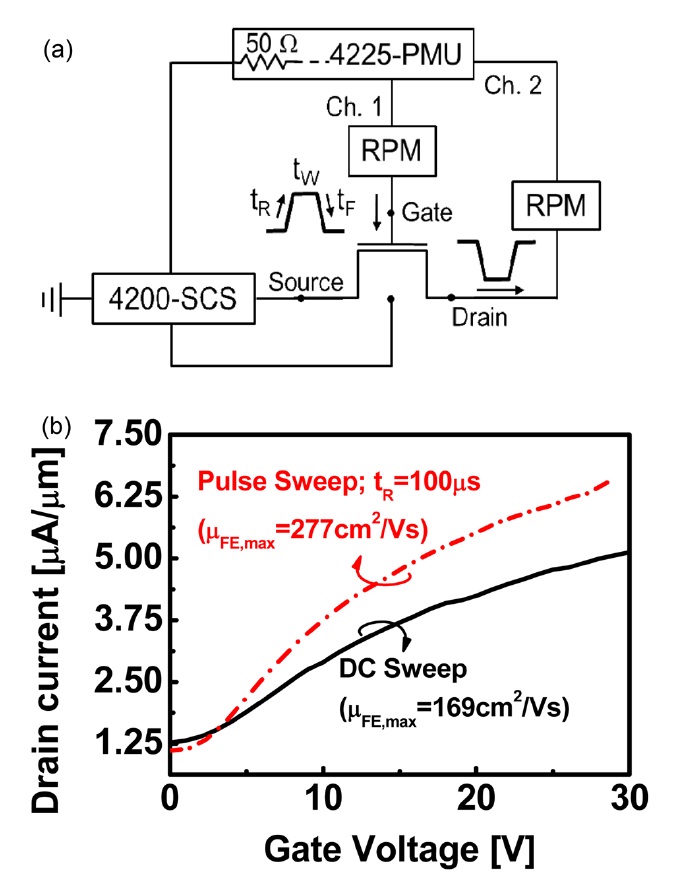
High speed I-V measurements can eliminate the influence of charge trapping and self heating. Lee et al. [14], performed pulse I-V measurements on a graphene MOSFET (rise time = fall time = 100 μsec, pulse width = 10 msec) (Fig. 4a) and demonstrated a 64% enhancement in field effect mobility (Fig. 4b). However, it is known that tunneling-induced charge trapping can occur even below one microsecond. Thus, Lee’s work is not completely free
from charge trapping. One limitation of the pulse I-V method is device impedance. To apply a shorter pulse, the impedance should be minimized, i.e., a short channel device is needed. The minimum pulse width to avoid the self-heating effect in a graphene device has not been studied yet. Since a 10 nsec pulse was needed to avoid the self-heating in a SOI device with a 30 nm silicon layer, graphene may require a much shorter device due to the extremely thin channel (0.34 nm).
Another possible approach to reduce the device scattering is using a very small channel length to avoid the influences of defects and charge puddles. Note that shorter channel devices and higher carrier concentrations tend to yield higher field effect mobility [35]. Unfortunately, due to the carrier scattering from edge states, scaling of width would have to be limited to tens of nm.
Potential sources of errors in the electrical characterization of graphene devices have been discussed. Clearly, the simple I-V curves of silicon devices need more careful considerations to extract intrinsic parameters from experimental data. With graphene, many factors that can influence the device characteristic are still unknown. Without a systematic study of those factors, the validity of electrical data extracted from graphene cannot be considered accurate enough. Thus, data reported in the literature should be taken with caution, as the majority of publications don't take any precautions to improve the quality of electrical data.