In this work, we present a study regarding the etching characteristics on titanium nitride (TiN) thin films using an inductively coupled plasma system. The TiN thin film was etched using a N2/BCl3/Ar plasma. The studied etching parameters were the gas mixing ratio, the radio frequency (RF) power, the direct current (DC)-bias voltages, and the process pressures. The baseline conditions were as follows: RF power = 500 W, DC-bias voltage = -150 V, substrate temperature = 40℃, and process pressure = 15 mTorr. The maximum etch rate and the selectivity of the TiN to the SiO2 thin film were 62.38 nm/min and 5.7, respectively. The X-ray photoelectron spectroscopy results showed no accumulation of etching byproducts from the etched surface of the TiN thin film. Based on the experimental results,the etched TiN thin film was obtained by the chemical etching found in the reactive ion etching mechanism.
The dimensions of memory devices have been continuously shrinking in order to obtain higher speed and stability. As a result,this trend has led to research on leakage currents and low device conductivity. Device structures and process technology have approached their limits needed to improve the device characteristics and integration [1,2], leading to many studies regarding new structures and materials in order to address these problems. Titanium nitride (TiN) has been studied as an attractive material due to its many advantages. TiN thin films have low resistivity, a low diffusion coefficient, chemical stability, a good hardness, and a high compatibility with high-
There have already been many studies regarding the etching characteristics of TiN thin films. Chiu et al. [9] investigated the etching characteristics of TiN thin films in Cl2 and C2F6 gases.They showed that as the density of the Cl radicals increased the sidewall slope decreased, whereas as the density of the F radicals increased the sidewall slope increased. The research paper investigated the etching characteristics of TiN thin films in a Cl2/BCl3/Ar plasma. They showed the effect of the BCl3 plasma on the sidewall slope as the BCl3 gas increased [10]. As the flow rate of BCl3 gas increased the sidewall slope decreased. However, there are only a few studies related to TiN thin films using the dry etching method employing high density plasma sources favored by modern microelectronic technology. As a result, the influence of the input process parameters on the TiN etch rate have not been explored in detail, and the TiN etching mechanism remains unclear.
In this study, we investigated the etching characteristics and mechanisms of TiN thin films using N2/BCl3/Ar mixtures in an inductively coupled plasma (ICP) system. The chemical reaction
on the surface of the etched TiN thin film was investigated using X-ray photoelectron spectroscopy (XPS).
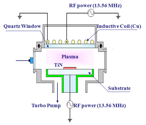
The TiN thin films were deposited on a SiO2 (100 nm)/Si substrate using atomic layer deposition. The total thicknesses of the TiN thin films were about 200 nm. The dry etching process was performed using an ICP system, as shown schematically in Fig.1. The reactor chamber was made from aluminum; the inner walls were anodized. A 3.5 turn spiral induction coil was located above a 24-mm-thick horizontal quartz window that separated the coil from the process chamber. The top copper coil was operated using 13.56 MHz radio frequency (RF) power; the bottom electrode was connected to another 13.56 MHz asymmetric RF generator in order to control the direct current (DC)-bias voltage.The distance between the quartz window and the substrate electrode was 9 cm. The chamber was evacuated to 10-6 torr using a mechanical pump and a turbo molecular pump. The baseline
conditions were: an RF power of 500 W, a DC-bias voltage of -150 V, a process pressure of 15 mTorr, and a substrate temperature of 40℃. The TiN thin films were etched using N2/BCl3/Ar plasma.The etch rates were measured using a depth profiler (KLA Tencor,α-step 500; San Jose, CA, USA). The chemical reactions on the surfaces of the etched TiN thin films were evaluated using XPS (Thermo VG, Sigma Probe; East Grinstead, West Sussex, England).The source used for the XPS analysis was Al Kα with a spot size of 400 ㎛. The energy step size was 0.1 eV.
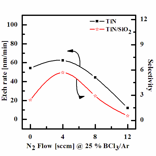
Figure 2 shows the etch rate of the TiN thin films and its selectivity to SiO2 as a function of the N2/BCl3/Ar gas mixing ratio at a process pressure of 15 mTorr, an RF power of 500 W, a DCbias voltage of -150 V, and a substrate temperature of 40℃. It can be seen that as the N2 (4 sccm) content in the BCl3/Ar plasma increased, the etch rate of the TiN thin film also increased, reaching a maximum of 62.38 nm/min at a N2 (4 sccm)/ BCl3 (25%)/Ar(75%) gas mixing ratio. The etch rates of the TiN thin film in BCl3(25%)/Ar (75%) and N2 (12 sccm)/BCl3 (25%)/Ar (75%) plasmas were found to be 54.2 nm/min and 12.13 nm/min, respectively.These findings support the assumption that, for a given range of experimental conditions, increasing the chemical reaction gas concentration decreases the etch rate. The selectivity of the TiN to the SiO2 increased from 2.42 to 5.70 until a N2 (4 sccm)/ BCl3(25%)/Ar (75%) plasma was used. The result was a lowering in the rate of the chemical reaction in the BCl3-rich plasma due to the deposition of solid inorganic compounds which were the result of the complete dissociation of the BCl3 molecules. It can be seen that the variation in the gas mixing ratio caused monotonic changes in the electron density, the electron temperature, the total ion density, and the N atom density. Accordingly, we can assume the same monotonic behaviors can be found in the fluxes of these species, and the first of the proposed mechanisms can be ignored. It is our opinion that the second and third mechanisms operate simultaneously.
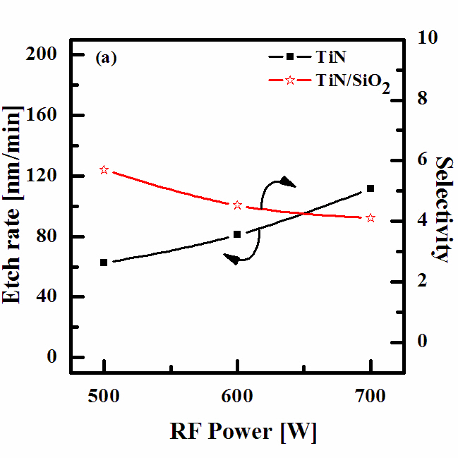
Figure 3 shows the etch rate of the TiN thin films and the selectivity of the TiN to SiO2 as a function of the RF power for the N2 (4 sccm)/BCl3 (25%)/Ar (75%) plasma. As the RF power increased,
the TiN etch rate increased from 62.38 nm/min at 500 W to 111.5 nm/min at 700 W; the selectivity of TiN to SiO2 decreased from 5.7 to 4.12. An increase in the RF power causes monotonic increases in both the dissociation and the ionization rates, and thus in the densities and fluxes of the N atoms and positive ions. In our case,such a layer can result from the deposition of solid N which then bonded with the surface oxygen in order to form ClxNy, as well as from the N and Cl radicals incorporated into the polymer-like structure.
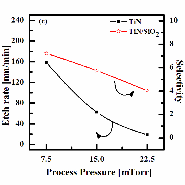
Figure 4 shows the etch rate of the TiN thin films and the selectivity of the TiN to SiO2 as a function of the process pressure for the N2 (4 sccm)/BCl3 (25%)/Ar (75%) gas mixing ratio. As the pressure increased from 7.5 mTorr to 22.5 mTorr, the TiN etch rate decreased from 158.25 nm/min to 18.68 nm/min. The selectivity of the TiN to SiO2 also decreased, from 7.23 to 4.04. In our opinion, the effect of the gas pressure on these parameters is as follows. An increase in the gas pressure enhances the density of the neutral chemically active species but lowers the ion mean free path and ion energy. As a result, with an increasing gas pressure,there is a tendency toward acceleration in the chemical etch pathway but a worsening for the ion stimulated desorption of the reaction products, which likely results in a decreased fraction of the free surface acceptable for the chemical reaction. Similar to the effect of the gas mixing ratio, these two factors work in opposing directions, producing a non-monotonic behavior in the etch rate.
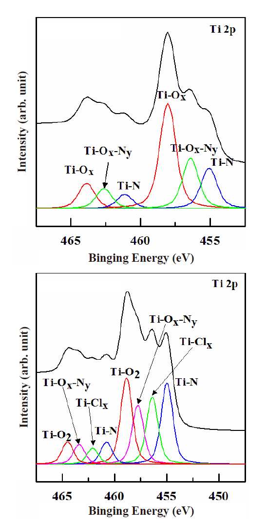
Figure 5 shows the Ti 2p peaks of the XPS narrow scan spectra used to investigate the chemical etch characteristics of the TiN thin film on the surface. The process conditions were 500 W for the RF power, -150 V for the DC-bias voltage, 15 mTorr for the process pressure and 40℃ for the substrate temperature. Figure 5(a) shows the Ti 2p peaks of the XPS narrow scan spectra in the as-deposited TiN film. Three peaks were found for this condition.The Ti-O2 bond was 458 eV, the Ti-Ox-Ny bond was 456.5 eV, and the Ti-N bond was 455 eV. The oxygen is assumed to be injected during the deposition process. Figure 5(b) shows the Ti 2p peaks of the XPS narrow scan spectra when using N2/BCl3/Ar plasma.The gas mixing ratio was N2 (4 sccm)/BCl3 (25%)/Ar (75%). A new peak appeared at 455.8 eV. This peak is thought to be made up of non-volatile Ti-Clx compounds. This can be explained by the ions bonds being weakened during the decomposition and recombination occurring during the physical sputtering. The physical etch was increased by the N2 addition and so it could assist in evaporating the nonvolatile compounds on the surface.However, the B radical amounts were reduced in the plasma by the N2 addition. This can explain why recombination occurred more strongly after decomposition.
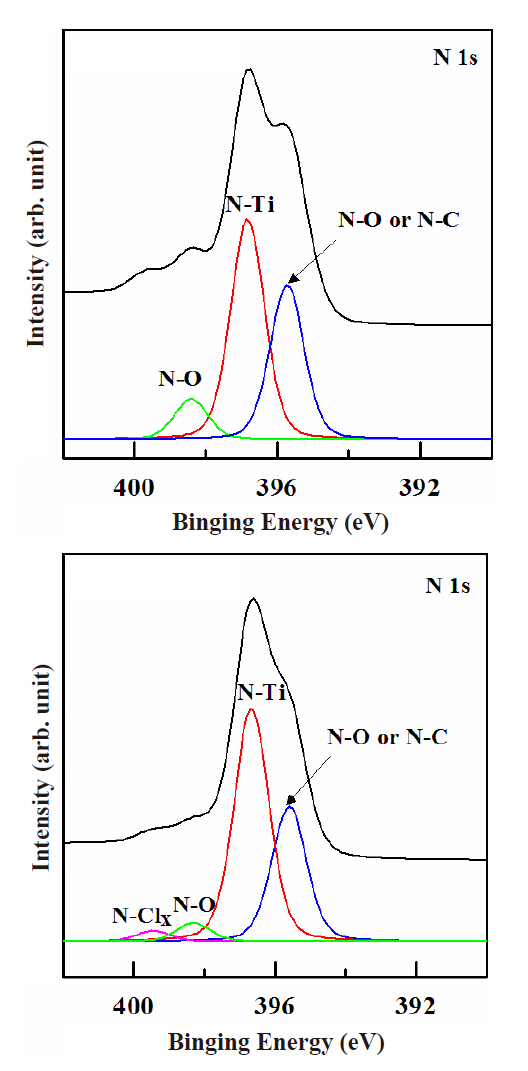
Figure 6 shows the N 1s peaks of the XPS narrow scan spectra.The process conditions were 500 W for the RF power, -150 V for the DC-bias voltage, 15 mTorr for the process pressure, and 40℃for the substrate temperature. Figure 6(a) shows the N 1s peaks of XPS narrow scan spectra in the as-deposited TiN film. Three peaks are seen in Fig. 6(a): N-Ti, N-O, and N-C compounds.Figure 6(b) shows the N 1s peaks of XPS narrow scan spectra for the N2/BCl3/Ar plasma treatment. The gas mixing ratio was N2(4 sccm)/BCl3 (25%)/Ar (75%). The intensity of the N-O and N-C peaks was decreased. This can be explained by the O and N radicals breaking their bonding by Ar ions sputtering and evaporated during the etch process. A new peak was found at 399 eV, this peak is thought to be caused by the N-Cl compounds from the BCl3 plasma. The intensity of each peak was decreased. This can be explained by the fact that N- bonds can be easily broken by the N2 addition to the BCl3/Ar plasma [11-13].
In this study, we carried out experimental investigations into the TiN thin film etching mechanisms in N2/BCl3/Ar plasma. We found that an increase of the N2 content in the BCl3/Ar plasma leads to an increase in the TiN etch rate, which reaches a maximum value of 62.38 nm/min at a concentration of 4 sccm N2 because a large addition of N2 to the BCl3/Ar plasma increases the chemical reaction effect. Due to the relative volatility of the by-products formed during the N2/BCl3/Ar plasma etching, ion bombardment was required in addition to physical sputtering in order to obtain these high TiN etch rates. The reason for this etch rate maximum is due to the concurrence of both physical and chemical pathways in the ion-assisted physical reaction. Volatile oxygen compounds identified in the XPS results indicate that Ti 2p and N 1s form non-volatile metal chlorides and volatile boron-oxy-chlorides. These results agree with the universal energy dependency of the ion enhanced chemical etching yields.