Recently, a spin-orbit (SO) interaction observed in narrow-gap semiconductor heterojunctions has attracted much attention,since it can provide a basic operation principle for various novel spintronics devices, such as spin-filters and spin field-effect transistors (spin FETs). The concept of the spin-FET is based on the SO coupling in the two dimensional electron gas (2DEG)causing a Rashba spin precession which can be controlled by a gate voltage [1]. Spin-injection and detection are carried out by ferromagnetic (FM) electrodes. As candidate structures for Rashba effect based spin-FET devices, various high electron mobility transistor (HEMT) structures have been studied [2,3]. The Rashba mechanism has been found to be especially enhanced in narrow gap InAs-based heterostructures [4].
Our recent investigations into the SO interaction in higher Incontent(~75%) InGaAs 2DEGs have shown a very large Rashba SO interaction coupling constant, α~ 30 × 10-12 eVm, in the normal-HEMT (n-HEMT) structure [5]. As used here, α describes the sensitivity of the spin precession when the electron travels across the electric field (E) at the heterointerface; it is roughly proportional to ~ (1/m*Eg) <E>), where m* is the electron effective mass, Eg is the bandgap energy, and <E> is the expectation value of the electric field E normal to the interface. Therefore, the α value can be determined by the materials selected and the specific design of the modulation-doped heterostructure. The above value of αis large enough to control the spin precession, since the value gives a π rotation length (lπ = πh2/2 m* α) of ≤0.2 ㎛. In contrast,highly efficient spin injections/detections have not been clearly attained, such as in n- and/or relatively thick channel inverted-HEMT (i-HEMT) structures with FM/semiconductor (S) or FM/insulator (I)/S electrodes. From the viewpoint of obtaining realistic Rashba-type spin-injection devices, with a strong SO interaction as well as the possibility of realizing a high spin injection efficiency,we focused on inverted InGaAs/InAlAs structures which possess a thin and low potential barrier between the surface FM and the 2DEG. The Rashba effect in such thin channel i-HEMT structures, however, has not yet been sufficiently clarified.
In this work, molecular beam epitaxy growth of the In0.5Ga0.5As/In0.5Al0.5As thin channel (≤60 nm) narrow-gap i-HEMT interface
and the transport analysis results of the 2DEG confined at the heterointerface are herein reported. The analysis includes the characterization of the in-plane transport as well as the Rashba SO interaction investigated by measuring the Hall effect and magnetoresistance (MR) oscillations in the van der Pauw and Hall bar samples using three kindred in-plane current directions([110], [1-10] and [100]). In the analysis, we focused on the dependency of the low temperature 2DEG mobility and the SO coupling constant (α) upon the different HEMT types (inverted or normal) and the In0.5Ga0.5As channel layer thickness. We also paid attention to the effects of the very thin In0.5Al0.5As cap layer.
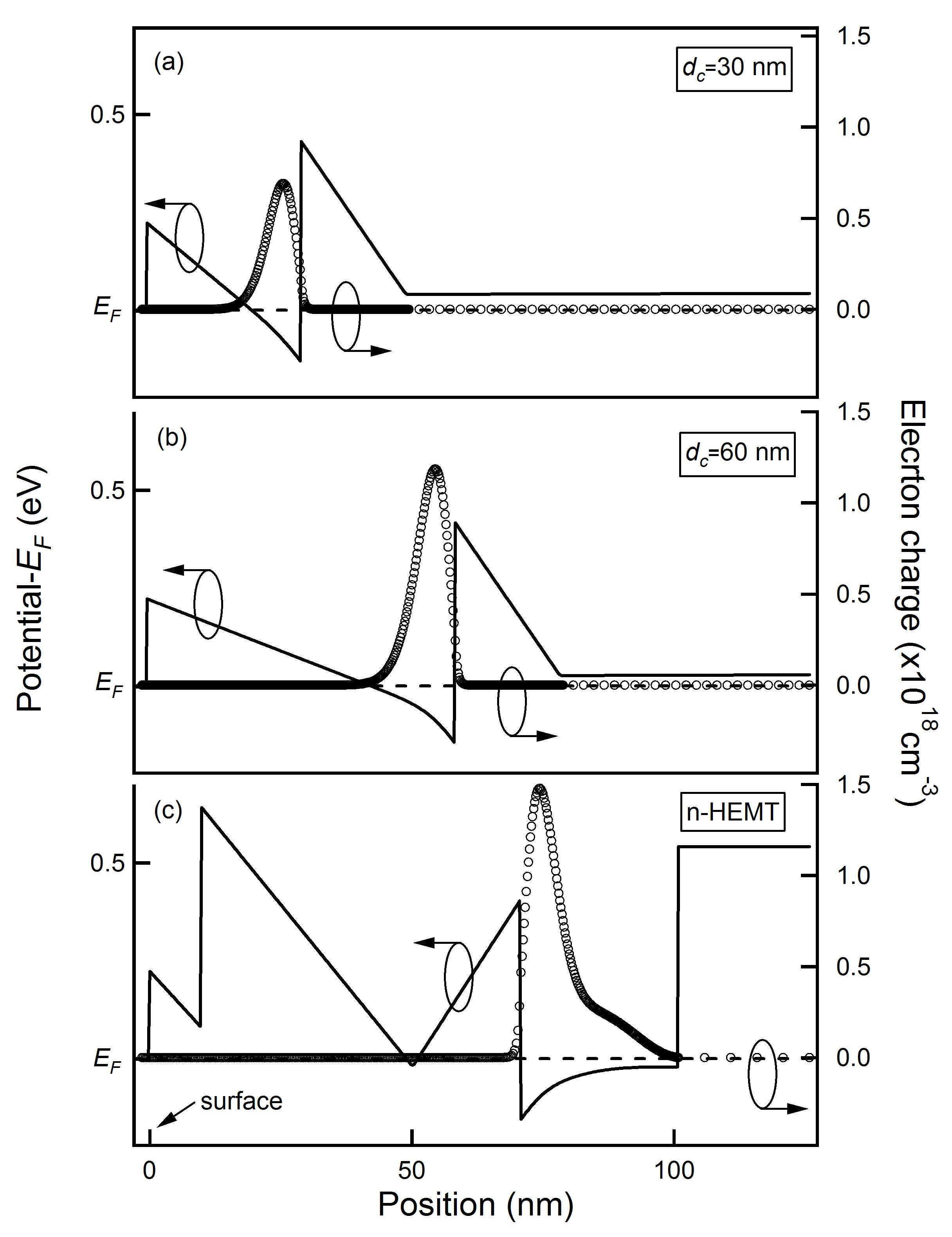
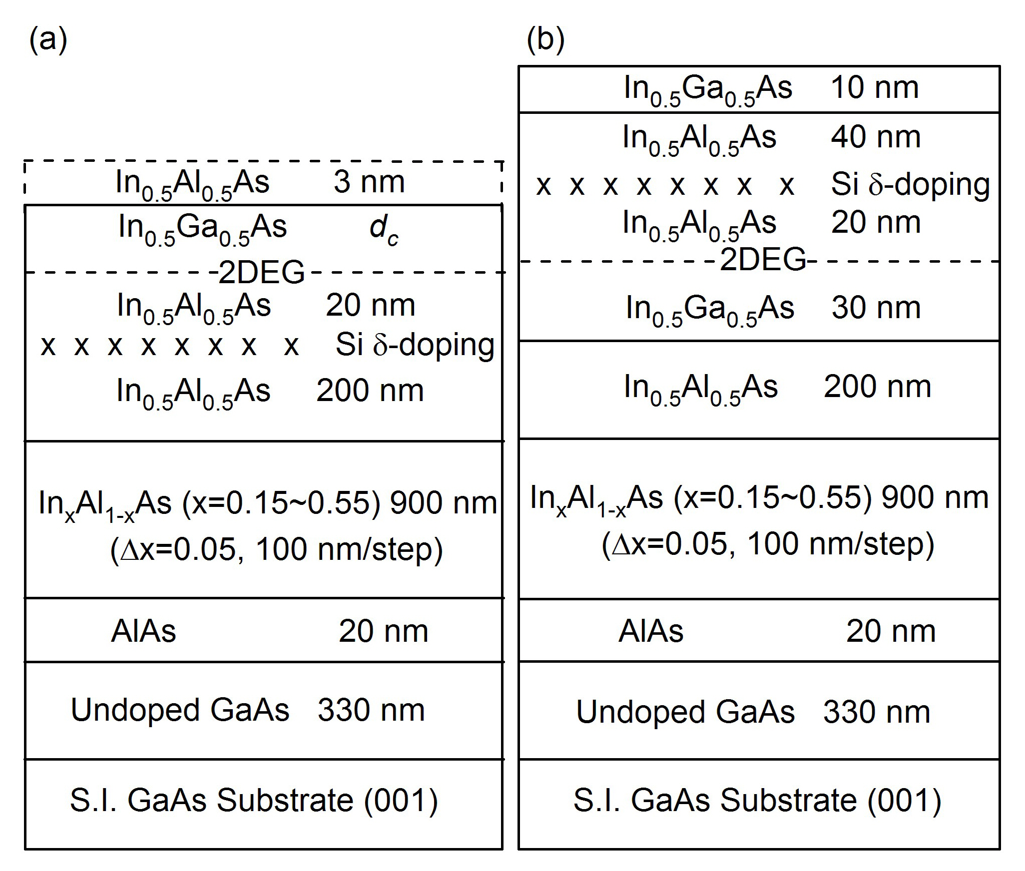
The samples used in this study were grown on semi-insulating GaAs (100) substrates using a conventional molecular beam epitaxy(MBE) apparatus. Prior to the growth, an oxide desorption was carried out under As4 flux at a beam equivalent pressure of 1.3× 10⁻⁵Torr. The surface oxide desorption process involved slowly ramping up the substrate temperature at a rate of 20℃/min until the reflection high-energy electron diffraction pattern showed a clear 2 × 4 surface reconstruction. This surface reconstruction transformation was adopted as a means to calibrate the substrate temperature, which was set at ~590℃, as measured by an infrared pyrometer. Four different i-HEMT structures were designed and grown in order to investigate the In0.5Ga0.5As channel thickness dependency on the spin-related transport properties and the effects of the very thin In0.5Al0.5As cap layer. An n-HEMT structure was also grown as a reference. The layer structures of the grown samples are shown in Fig. 1 and the corresponding conduction band profiles and charge distributions calculated by taking into account the structure and doping conditions adopted in the growths are shown in Fig. 2. Before depositing the modulated doping heterostructure, the substrate temperature of 350℃,selected to reduce the dislocation that occurs during the growth of the step graded InxAl1-xAs buffer (which has good isolation properties; its final inverse step was adopted in order to reduce the residual strain), was increased up to 450℃ to avoid te point defects that can result from the excess arsenic atoms [6]. The silicon δ-doping density was fixed at ~7 × 1012 cm-2. The channel In0.5Ga0.5As layer was separated by a 20 nm thickness undoped In0.5Al0.5As spacer in order to reduce the remote ionized donor
scattering. Figure 1(a) shows the inverted In0.5Ga0.5As/ In0.5Al0.5As HEMT structure with the two different channel thicknesses (dc= 30 nm and 60 nm). For the final growth step, an undoped 3 nm In0.5Al0.5As cap-layer was grown after the In0.5Ga0.5As channel deposition. Figure 1(b) shows a normal In0.5Ga0.5As/In0.5Al0.5As HEMT structure grown under similar conditions as a reference. For the spin transport analysis, regular van der Pauw (size = 5 ×5 mm2) and Hall bar samples (channel length = 50 ㎛ and width= 200 ㎛ with three different channel directions [1-10], [110] and [100]) were prepared by photolithography. The SO coupling constant, α, was determined using fast Fourier transformation(FFT); the beating nodes Landau plot of the oscillations was observed in the low field Shubnikov-de Haas (SdH) signals at ~1.5 K.Alternatively, the SO coupling constant was also extracted from the analysis of weak anti-localization (WAL) for dc = 30 nm both with and without cap samples, which have a low mobility and a strong SO interaction.
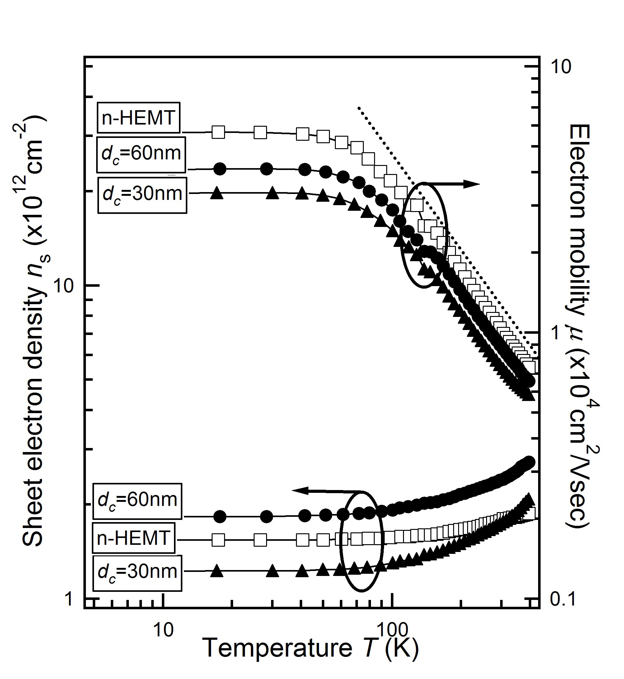
The van der Pauw samples were initially characterized by Hall measurements. Figure 3 shows the temperature dependencies of the sheet electron density (ns) and the electron mobility (μ) for the i-HEMT (dc = 30 and 60 nm with cap-layer [WC]) samples and also for the n-HEMT. In the high temperature region, μ is limited by phonon scattering and proportional to the T-2/3 line. Conversely,it was found that the saturated value of the low temperatureμ decreases when dc decreases. It is thought that alloy scattering as well as surface charge scattering are the primary mechanisms limiting the μ in the i-HEMT structure [7]. Since the alloy scattering should be almost equal between the two i-HEMT samples of
dc = 30 and 60 nm, the increase of the surface charge scattering might be responsible for the decrease of the mobility in the dc =30 nm sample. That is, the surface charge is closer to the 2DEG in the dc = 30 nm sample than in the dc = 60 nm sample.
Figure 4 shows the second derivatives (d2Rxx/dB2) of the low field MR (Rxx) oscillations in the Hall bar samples for the different current directions, [1-10], [110] and [100], for the (a) dc = 60 nm sample and the (b) dc = 30 nm sample without a cap-layer (WOC).The insets show the FFT of the [1-10]d2Rxx/dB2 oscillations carried out to estimate the Rashba SO coupling constant (α) [5]. In the WOC dc = 60 nm i-HEMT sample, clear beating patterns can be seen and the node positions are depicted by vertical arrows.From the beating period ΔB-1 = 0.30 (T-1) in the WOC case, we can determine the α values of ~12 × 10-12 eVm by Schapers et al. [8]:
Where, m* = 0.06 m0 is the non-parabolic effective mass, kf is the Fermi wave number and Δi is the node index unit difference.In the traces seen in Fig. 4(b), however, the beating patterns are not as clear as those seen in Fig. 4(a). This is probably a result from the relatively low electron mobility in the samples. Since the beating periods in themselves are not sufficient to estimateα, we have utilized the corresponding FFT results (the insets) and the values are roughly estimated to be ~20 × 10-12 eVm for the α =30 nm sample. Contrarily, the α value in the n-HEMT is estimated to be < 5 × 10-12 eVm. Another interesting conclusion indicated
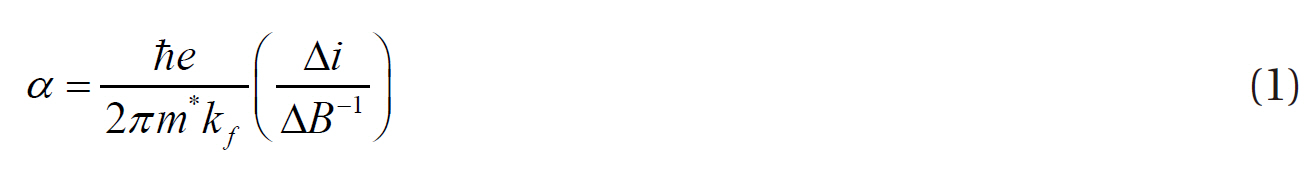
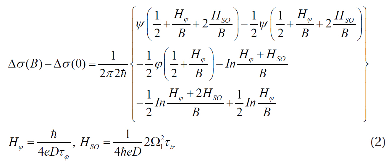
from the traces is that there is almost no in-plane anisotropy for the beating oscillation period, suggesting that there is no inplane anisotropy for α as well. The WAL effect, an alternative and complementary method, was applied to the dc = 30 nm samples;the α values are determined by the following Iordanskii et al. [9]equation in the case that only the Rashba term is present:
Here, Ψ is the digamma function, D = vF 2τtr/2 is the diffusion constant, vF = ħkf/m* is the Fermi velocity, and τtr = ㎛*/e is the transport relaxation time. These parameters were obtained from the Hall and SdH measurements. For the conductivity correction
Δσ(B)- Δσ(0), two adjustable parameters were used to fit the experimental data with this model: Hφ, the magnetic field related to the phase coherent relaxation time τφ, and HSO, the magnetic field related to the half of spin splitting energy Ω1.
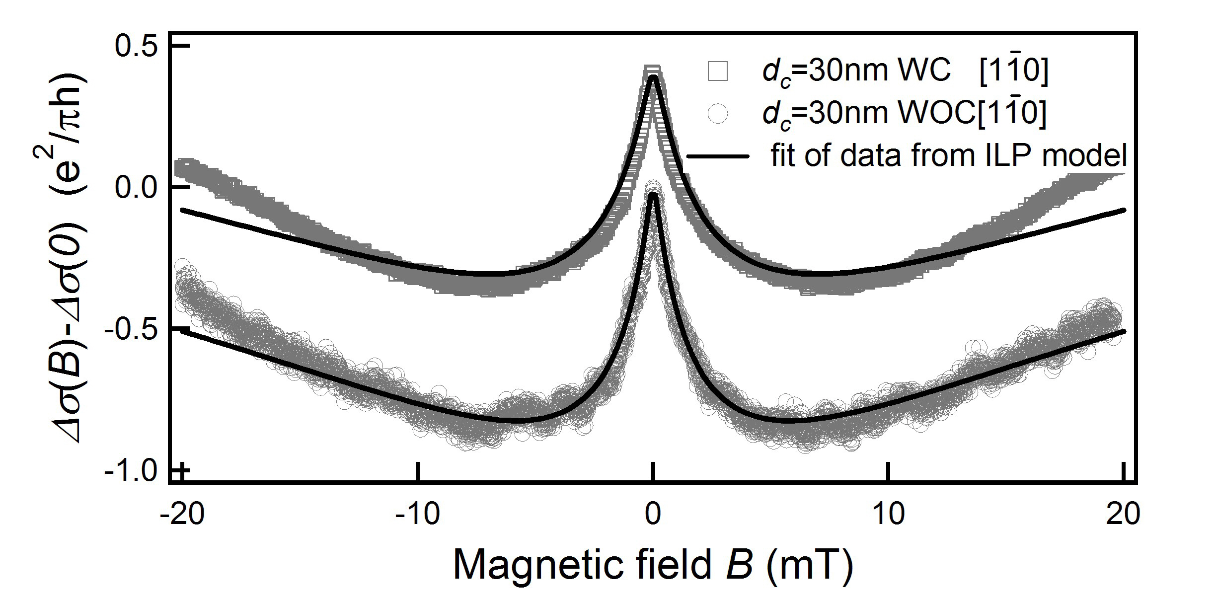
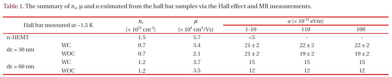
Figure 5 presents the experimental data of conductivity correction for the dc = 30 nm WC and WOC samples compared to the calculated curve obtained from the Iordanskii equation. The results of the curve fitting are τφ = 8 ps and Ω1 = 8 × 10-23 J, respectively.From the Ω1 = α kf relation we derive α ~2.4 × 10⁻¹² eVm values. However, this α is very small when compared to the value(~20 × 10-12 eVm) obtained from the SdH oscillation beating patterns.In other words, the WAL analysis is difficult to apply to this kind of sample, which has a strong Rashba SO interaction giving the relation τSO < τtr. Table 1 summarizes the results of the Hall measurements and the α analysis in the Hall bar samples. One thing to note is that in the 30 nm samples the cap layer formation was found to definitely effect the mobility of the confined 2DEG. We obtained a ~50% higher mobility 2DEG even with a clear beating signal in the SdH oscillations in the WC sample when compared to the WOC sample. This is mainly due to the proper Fermi-level pinning at the wafer surface by the cap layer.In such a case, the suppression of the above-mentioned surface charge scattering is expected. It is also noted that since the cap layer is sufficiently thin, it does not become a totally transparent tunnel barrier for the injection electrons. Another thing to be noted is that the α value is larger in the i-HEMT samples than that found in the n-HEMT sample and is larger also in the thinner dc = 30 nm sample than in the dc = 60 nm sample. This is probably due to the difference in the triangular potential well between these HEMT samples. Actually, from the calculated results from Fig. 2, it was estimated that the mean electric field strength at the heterointerfaces of the dc = 30 nm, 60 nm and n-HEMT samples, <Edc = 30 nm>, <Edc = 60 nm>, and <En-HEMT>, are approximately 1.3, 0.9 and 0.45 (×105 V/m), respectively. Since α is essentially proportional to the strength of the electric field at the well bottom, the decrease of α in the n-HEMT and in the thicker dc samples can be attributed to the decrease of <E>. So that, the thin (dc = 30 nm) channel i-HEMT samples (with the InAlAs cap),as described here, could be one of the promising spin-FET base materials when the FM electrodes are formed on the surface with well-defined interface structures.
We investigated the basic electronic properties as well as the magnitude and in-plane anisotropy of the Rashba SO interaction in thin channel In0.5Ga0.5As/In0.5Al0.5As i-HEMTs. The low temperature mobility of the 2DEG decreased with a decrease in the thickness of the In0.5Ga0.5As channel layer. In addition, the low temperature mobility of the 2DEG in the sample with thin In0.5Ga0.5As channels is found to be improved by adding a very thin undoped In0.5Al0.5As cap layer onto the top of the layered structure. The former is considered to be due to the increase of the surface charge scattering in the thinner channel sample and the latter probably originates from the suppression of the scattering by the Fermi level pinning with the cap layer. The structural dependent characteristic of the Rashba spin transport was observed through the low temperature magneto resistance and weak anti localization measurements. We determined that a WAL analysis is difficult to apply to a high mobility sample that has a strong Rashba SO interaction giving the relation τSO < τtr. Consequently,a larger α is confirmed in the i-HEMTs than that found in the reference n-HEMT; the α value likely increases with a decreasing channel layer thickness dc, probably due to the increase of the interface electric field strength caused by the increase of the asymmetry of the well potential. In addition there are almost no in-plane anisotropies for ns, μ and α in the 2DEG confined in the thin channel i-HEMT samples.


![The magnetoresistance (MR) results for the (a) dc = 60 nm without a cap-layer (WOC) samples and for the (b) dc = 30 nm WOC samples with different current directions. The inset shows the fast Fourier transform result for the [1-10] MR oscillation.](http://oak.go.kr/repository/journal/10914/E1TEAO_2011_v12n4_140_f004.jpg)
![The conductivity correction fitting plotted as a function of the magnetic field for the dc = 30 nm with cap-layer (WC) and without cap-layer (WOC) samples in the [1-10] direction. The experimental data are given by the circles and the calculated fitting curve is represented by the solid curve.](http://oak.go.kr/repository/journal/10914/E1TEAO_2011_v12n4_140_f005.jpg)