Complementary metal-oxide-semiconductor (CMOS) technology can be a very powerful solution for optical receivers[1]. It can provide cost-effective and high-volume fabrication as well as single chip integration of the photodetector and electronic circuits, all of which can be of great advantage for realization of high-performance, low-cost optical interconnects. However, there are inherent drawbacks of CMOS technology for photodetector applications. In particular, the narrow depletion width of PN junctions in CMOS technology causes photodetector performance degradation. Several attempts have been made to overcome this drawback. Additional lowdoped layers or silicon-on-insulator technique have been considered [2, 3], but these require additional fabrication costs. As an attempt for realizing high-speed and highresponsivity photodetectors with standard CMOS technology without any process modification, we have investigated CMOS-compatible avalanche photodetectors (CMOS-APDs)based on P+/N-well and N+/P-well junctions [4, 5].
In general, in spite of their low-bandwidth characteristic, N-well/P-substrate junctions have been used for high-sensitivity photodetectors in standard CMOS technology because the depletion width is relatively larger than other junctions resulting in high responsivity. In this work, we report the results of a comparison study of CMOS-APDs based on two types of PN junctions, N-well/P-substrate (NP-type)and P+/N-well (PN-type) junctions. Their current-voltage characteristics, responsivity, avalanche gain, and photodetection bandwidth are investigated and analyzed. By comparing two types of CMOS-APDs, the important factors influencing CMOS-APD performance are identified.
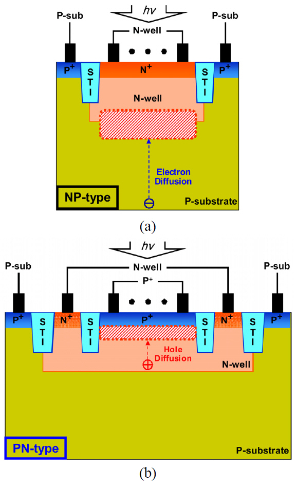
Fig. 1 shows cross sections of two types of CMOS-APDs fabricated with 0.13-㎛ standard CMOS technology. In NP-type, the vertical PN junction between N-well and P-substrate is used for photodetection, and in PN-type, the PN junction between P+ source/drain and N-well. Both types include shallow trench isolation (STI), which is generally used on standard CMOS technology to prevent current leakage between adjacent components and formed by depositing dielectric materials such as silicon dioxide into the shallow trench, between P+ and N+ regions. In PN-type, photocurrents are extracted from P+ contacts located inside N-well, and P+ contacts for the substrate are tied to ground in order to exclude any substrate influence. For both types, an optical window having the area of 30 by 30 ㎛2 is formed by blocking the salicide process. The total device area is 37.2 by 37.2 ㎛2 for NP-type and 43.8 by 43.8 ㎛2for PN-type. Both types of photodetectors can be realized without violating any design rule for the CMOS process technology [6].
For DC characterization of CMOS-APDs, an 850-nm laser diode was used as an optical source, and a lensed-fiber was used for injecting light into photodetectors on the wafer. For DC measurements, 0.1 mW of light measured at the lensed-fiber output was injected into photodetectors.
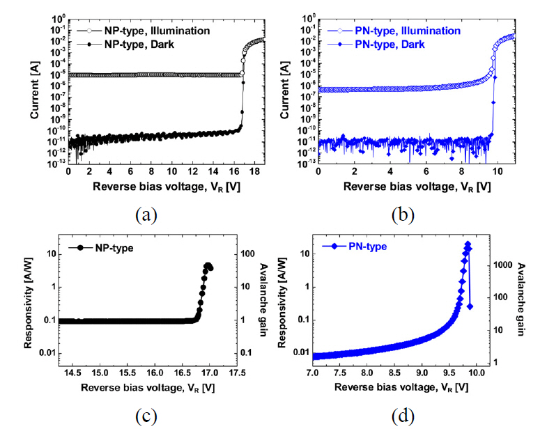
Fig. 2 (a) shows current-voltage characteristic of CMOSAPDs under illumination and dark conditions. The avalanche breakdown voltages of NP-type and PN-type CMOS-APDs are about 16.9 and 9.8 V, respectively. The difference in breakdown voltages is mostly due to the difference in doping concentrations. The doping concentration for P-substrate is less than N-well, resulting in larger breakdown voltage for NP-type. When the bias voltage is small, NP-type has much higher photocurrents. For example, at the reverse bias voltage of 1 V, NP-type has photocurrent of about 9.5 μA, whereas PN-type has 0.46 μA. This is because NP-type has larger drift currents with larger depletion width due to lower doping concentration for P-substrate as well as larger diffusion currents from larger volume of the charge neutral region in P-substrate than PN-type. However, as can be seen in Fig.2 (b), responsivity becomes higher for PN-type as the reverse bias voltage increases. For example, the peak responsivities of NP-type and PN-type CMOS-APDs are about 4.68 and 20.3 A/W, respectively. This difference is due to the influence of STI on the junction breakdown. In NP-type, breakdown occurs at the edges of the PN junction where the local electric field becomes higher due to junction curvature since STI does not penetrate deep enough to these junction edges. However, in PN-type, STI with much higher breakdown field strength [7] surrounds the junction edge and, consequently, breakdown occurs at the planar PNjunction where the curvature effect has less influence, resulting in higher breakdown field than NP-type. Consezquently, more avalanche gain can be obtained for PN-type, resulting in higher responsivity than NP-type as can be seen in Fig. 2(b). Beyond the peak avalanche gain voltage, avalanche gains of CMOS-APDs start to decrease due to enlarged dark currents.
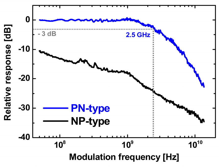
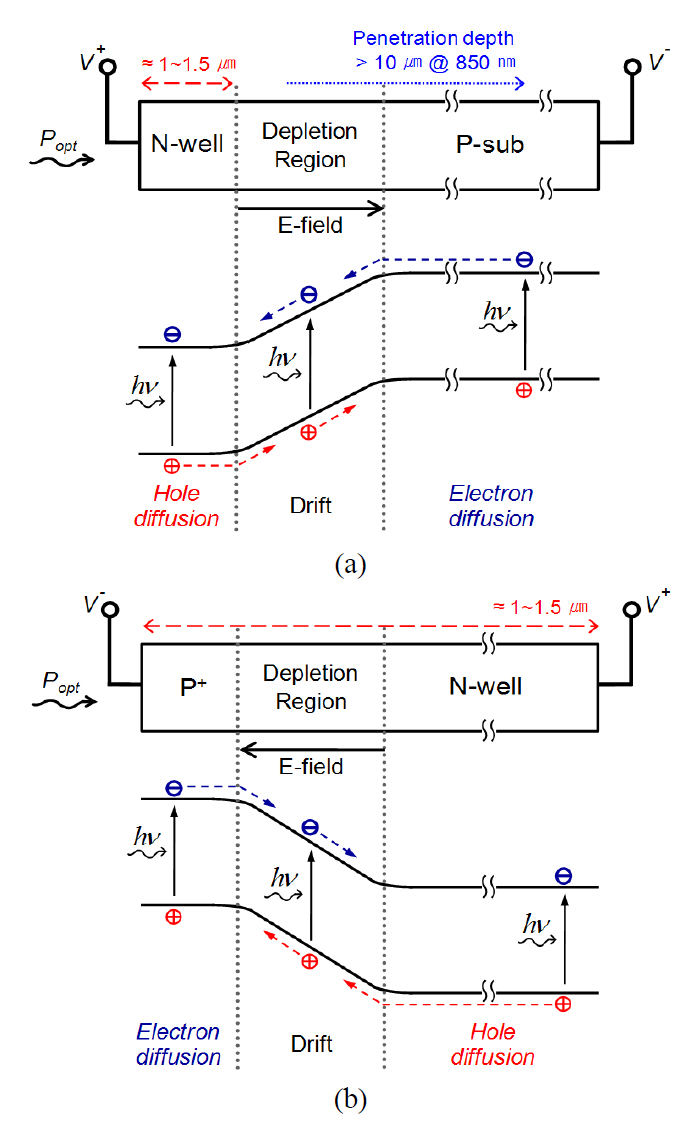
Fig. 3 shows photodetection frequency responses of CMOSAPDs. For this, an electro-optical modulator and a vector network analyzer were used with prior calibration of cables and RF adaptors. The average optical power injected into photodetectors was 1 mW. As can be seen in Fig. 3, PN-type CMOS-APD has much better frequency response. The reason can be well explained with Fig. 4, which shows simplified band diagrams for two types of CMOS-APDs. As shown in Fig. 4, in NP-type, many photons are absorbed in the charge neutral P-substrate region where no electric field exists, and photogenerated carriers reach the electrode by a slow diffusion process. In PN-type, however, the charge neutral N-well region is much smaller and, consequently, carrier transport by diffusion takes less time, resulting in better frequency response. The 3-dB bandwidth of 2.5 GHz for PN-type CMOSAPD allows several Gb/s-level all-CMOS integrated optical receivers [8].
Performances for two types of CMOS-APDs are compared. Several characteristics such as photocurrent, responsivity,avalanche gain, and photodetection bandwidth are experimentally investigated. Although NP-type CMOS-APD has high intrinsic responsivity, it cannot achieve high avalanche gain since it suffers from edge breakdown without STI. In addition, it has low bandwidth due to slow diffusion photogenerated carriers from P-substrate region. On the other hand, PN-type CMOS-APD has high responsivity due to large avalanche gain achieved with high breakdown field provided by STI and high photodetection bandwidth with less influence from slow diffusion of photogenerated carriers from P-substrate. From this study, it is clearly demonstrated that CMOS-APDs based P+/N-well junction can provide much better performance than those based on N-well/P-substrate junction.