We analyze the current density ? voltage (J ? V) curve of a Cu(In,Ga)Se2 (CIGS) thin-film solar cell measured at different irradiation power densities. For the solar-cell sample investigated in this study, the fill factor and power conversion efficiency decreased as the irradiation power density (IPD) increased in the range of 2 to 5 sun. Characteristic parameters of solar cell including the series resistance (rs), the shunt resistance (rsh), the photocurrent density (JL), the saturation current density (Js) of an ideal diode,and the coefficient (Cs) of the diode current due to electron-hole recombination via ionized traps at the p-n interface are determined from a theoretical fit to the experimental data of the J ? V curve using a two-diode model. As IPD increased, both rs and rsh decreased, but Cs increased.
Recently, the Cu(In,Ga)Se2 (CIGS) thin-film solar cell has been the subject of intensive research and development in the photovoltaic industry [1-6]. CIGS has a great potential for solar cells with high power-conversion efficiencies. The record efficiency for a small-size CIGS thin-film solar cell is about 20 % [1]. CIGS solar cells can also be fabricated on a wide-area substrate cost-effectively [3-4]. These advantages offer CIGS a possibility to achieve the grid parity to compete with conventional technologies. In order to fabricate a highly efficient CIGS solar cell, it is prerequisite to have knowledge of the properties of material and the characteristic circuit parameters of the solar cell.
In particular, the diode current (or the dark current), the series resistance, and the shunt resistance have significant effects on the performance of a solar cell [7]. The diode current is generated by electron-hole recombination occurring at the p-n interface or in the quasi-neutral regions of p-type and n-type semiconductors. The series resistance and the shunt resistance are known to be affected by various properties such as the quality of materials constituting the solar cell and the grid design of solar-cell modules. A solar cell that has a low series resistance, a large shunt resistance and a small coefficient of the diode current yields a high fill factor in its current density - voltage (J - V)curve and therefore exhibits a high value of the powerconversion efficiency. These parameters can be estimated from a theoretical fit to the J - V curve of the solar cell [8-9]. Two simple approaches are lumped circuit models using one diode or two diodes. The one-diode model incorporates the ideality factor of diode to account for the effect of electron-hole recombination which occurs at the p-n interface, whereas the two-diode model handles it using a separate component of diode current. The two-diode model has been known to be more accurate than the one-diode model [8].
The purpose of this study is to investigate the performance of CIGS thin-film solar cells in concentrated photovoltaic applications. In the past years, there have been some studies on using CIGS solar cells as power generators which might be operated under solar irradiation with a power density less than one sun [10]. However, to the best of authors’knowledge, few reports have been available on the performance of CIGS thin-film solar cells under solar irradiation with a power density higher than one sun. In this report, we analyze the J ? V curve of a CIGS thin-film solar cell under irradiation of solar power densities from 1.5 to 5.0 sun. Using a lumped circuit model with two diodes, we found that both the series resistance and the shunt resistance tended to decrease as irradiation power density (IPD) increased.We also found that a component of diode current which is contributed by electron-hole recombination through traps at the p-n interface to the diode current tended to increase with IPD.
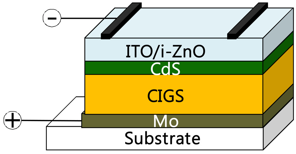
The structure of the CIGS thin-film solar cell prepared for this study is shown in Fig. 1. A Molybdenum film was coated as the back electrode on a soda-lime glass substrate,and CIGS with a thickness of about 2 ㎛ was deposited in a three-step evaporation process. Subsequently, CdS with a thickness of about 50 nm was formed by chemical vapor deposition (CBD), and intrinsic ZnO and indium-tine-oxide were deposited. Finally, fabrication of the current-collecting grid completed the device. The solar cell for this study had no anti-reflection coating. Fabrication of the solar cell is detailed elsewhere [11].
A solar simulator was used as the light source in J ? V measurements. The solar simulator provided an irradiation power density of 1 kW/m2 (AM1.5) at 25℃. The solar cell was mounted on a sample holder installed at a height
7.5 cm above an optical table. A power meter that is sensitive to the ultraviolet light was put in a position of 1.5 cm above the solar cell, and a convex lens was put above the power meter. We observed that the power of solar irradiation I is related to the distance between the lens and the power meter y within the focal length in the form I = I0 + k (y)2, where I0 and k are constants.This relation allowed us to find the position of lens for a desired power density on the solar cell. However, because the lens distorted the spectrum of lights passing through it,the spectra of the light through the lens was different from that without the lens. Therefore, in our discussion, we will exclude the J ? V curve measured at one-sun power density from comparison with others measured at different power densities. Since each measurement took about three seconds,we believe that an increase in the solar-cell temperature during each measurement did not change significantly the characteristic parameters of the solar cell.
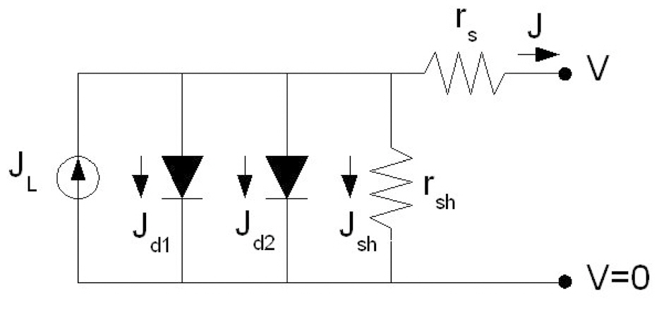
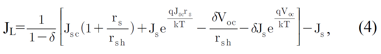
In order to determine the characteristic parameters of the solar cell, we employ a two-diode model whose equivalent circuit is shown in Figure 2. With this model, the J ? V curve can be obtained from the following equation:
where rs and rsh are the series resistance and the shunt resistance, respectively, in the unit of V/J. JL is the density of the photocurrent generated in the solar cell. Jd1 represents the diode current due to electron-hole recombination in the quasi-neutral region, and it is given as
where V'=V+Jrs is the applied bias across the depletion region of the solar cell, q denotes the fundamental electric charge, k is the Boltzmann constant, and T is the temperature in Kelvin. Js is the saturation current density of an ideal diode. Jd2 in Eq. (1) represents the diode
currents due to electron-hole recombination at the p-n interface of the solar cell, and it is given as [12]
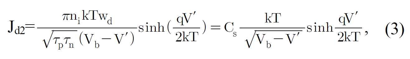
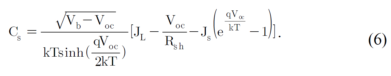
where ni is the intrinsic carrier density, and wd is the width of the depletion region. τp and τn are the shortest lifetime of hole and electron, respectively, when all the recombination centers at the p-n interface are filled with carriers of the opposite sign. It is noted that τp=1/Nt-σvp,th and τn=1/Nt+σvn,th, where Nt- and Nt+ are densities of negatively and positively charged traps, respectively. σ is the scattering cross section, and vp/n,th are the thermal velocities of hole/electron, respectively. qVb is the energy difference between the conduction-band edges of the p-type and n-type semiconductors at zero bias. In this study, we assumed Vb= 0.78V for the CIGS solar cell. In Eq. (3), some properties can be merged into Cs which represents the coefficient of Jd2. Thus, there are five parameters, JL, Js, Cs, rs, and rsh to be determined from the measured J ? V curve. We assume that these parameters do not depend on the bias voltage V.
However, since the short-circuit current density Jsc and the open-circuit voltage Voc can be determined easily from the experimental data, JL and Cs are expressed as functions of Jsc, Voc, Js, rs, and rsh :
where
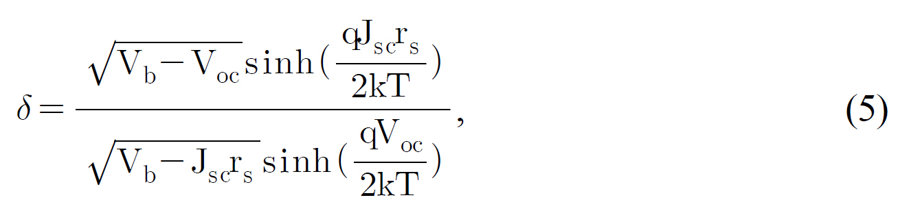
and
In order to fit Eq. (1) to the experimental result, we employ a numerical routine using three adjustable parameters,Js, rs, and rsh. In particular, as initial guesses for rs and rsh, we use 1/rs ='dJ/dV' at V = Voc and 1/rsh ='dJ/dV'at V = 0 which are estimated from the experimental data.
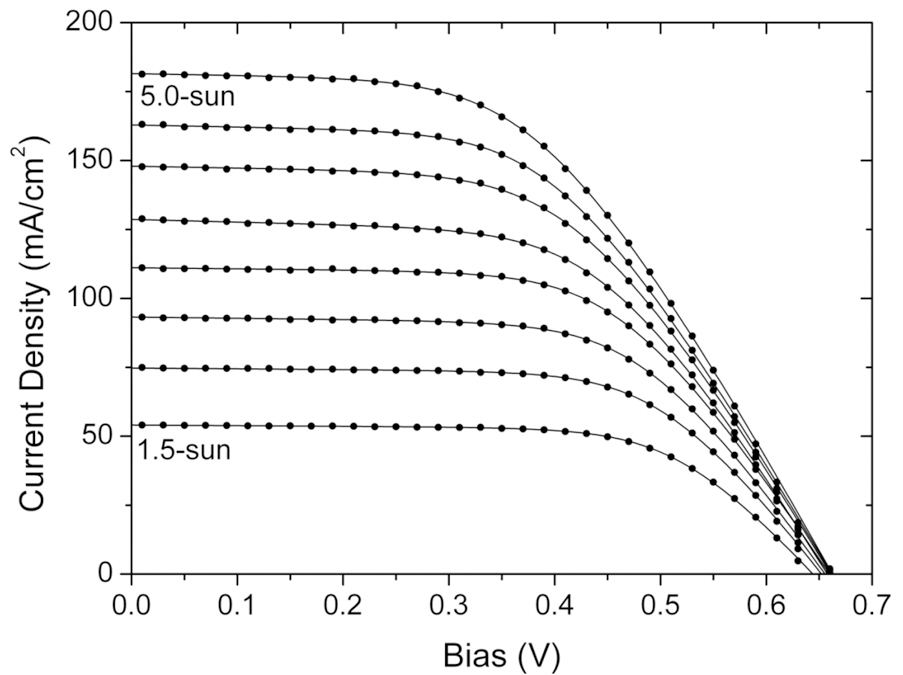
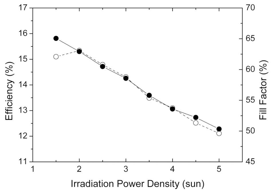
Figure 3 displays some J ? V curves of the solar cell under different irradiation conditions from 1.5 through 5-sun power density with a step of 1/2-sun power density. The dots
represent the experimental data, whereas the lines are the best theoretical fits to the experimental results in the range of bias between zero and the open-circuit voltage of each curve. For the best theoretical fit, we mean that the results of the fit were obtained by computer using a standard minimization routine of functions. Figure 4 plots the power-conversion efficiency and fill factor of the solar cell versus IPD. For our solar cell, the fill factor decreased monotonically from 65.1% to 50.3% as IPD increases from 1.5 to 5 sun. The power conversion efficiency increased with IPD in the range from 1.5 to 2 sun, but it decreased monotonically in the range from 2 to 5 sun. The maximum power conversion efficiency was 15.3% at an IPD of 2 sun.
In the rest of this article, let us attempt to explain why the power conversion efficiency decreased as IPD increased. For all the irradiation conditions of the J ? V curve shown

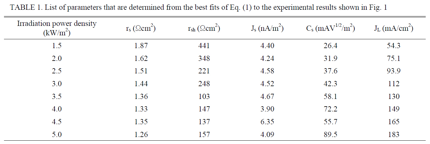
List of parameters that are determined from the best fits of Eq. (1) to the experimental results shown in Fig. 1
in Fig. 1, rs, rsh, Js, Cs, and JL which were determined from fits are listed in Table 1. It should be noted that since there are five adjustable parameters to fit experimental results, the parameters extracted from the fit may not accurately represent the properties of the solar cell, but the set of parameters obtained from a number of experimental results with different experimental conditions may show the correct behaviors of the parameters. Therefore, a few results whose values deviated greatly from the general behavior may be considered to have a large uncertainty in the numerical fit. JL is nearly proportional to IPD, which is obvious in the linear optical regime. Js does not show any dependence on IPD. This result indicates that the diffusion coefficient, diffusion length, and surface recombination velocities of minority carriers do not depend on IPD. However, for our solar cell, Cs is roughly proportional to IPD, implying that the density of the ionized traps which assisted electronhole recombination at the p-n interface increased as IPD increased. Because Cs is proportional to ,√Nt-Nt+ the density of diode current due to recombination at the p-n interface might increase with IPD. This causes a negative effect on the open-circuit voltage and the power-conversion efficiency.
On the other hand, rs and rsh decrease as IPD increases.The similar behaviors of rs and rsh were observed with CIGS thin-film solar cell under irradiation with a power density less than one sun [10]. The behaviors of rs and rsh of the solar cell under different irradiation conditions indicate that the conductivity of the materials constituting the solar cell and the number of shunt-current paths increased with IPD.However, our results show that the relative decrease of rsh is more rapid than that of rs as IPD increases from 1.5 to 5 sun. Since the density of defects plays an important role to determine the shunt resistance, we believe that an increase in the density of the ionized traps in the region of p-n junction with the increasing IPD gave an additional contribution to the decrease of rsh. This also provided one of reasons to reduce the fill factor and the power-conversion efficiency when IPD increases.
We have measured the J ? V curve of a CIGS thin-film solar cell under different irradiation conditions. Analyzing the J ? V curve using a two-diode model, we extracted the characteristic parameters of the solar cell. As IPD increased,the shunt resistance decreased more rapidly than the series resistance, whereas the coefficient of a diode current component due to electron-hole recombination at the p-n interface increased. These were two of reasons why the power conversion efficiency and the fill factor of the solar cell decreased when IPD increased.