Silicon photonics is widely regarded as a promising technology to meet the requirements of rapid bandwidth growth and energy-efficient on-chip communication while reducing cost per bit. In all potential application areas it is widely recognized that use of wavelength division multiplexing (WDM) techniques will be critical in achieving the required high levels of data transmission. Si photonics devices will have to deal with several tens of different wavelengths of light in the next-generation multi-core CMOS chips.
There are mainly four kinds of devices capable of multi/demultiplexing tens of WDM signals; they are ring resonators,lattice-form filters, arrayed waveguide gratings (AWG) and planar Echelle gratings. The former two are cascaded devices relying on temporal multi-beam interference effect and the latter two utilize spatial multi-beam interference effect. In order to achieve good crosstalk characteristics in the temporal and spatial multi-beam interference effects, uniformity of effective index nc(= β /k), where β and k denote propagation constant and wave number, is critically important.Filter characteristics of four kinds of devices will be investigated and performance limitations of silicon photonics filters are discussed.
In the latter part of the paper, an integrated-optic spectrometer based on Fourier-transform spectroscopy will be described. A novel planar waveguide spectrometer consists of interleaved Mach-Zehnder interferometer (MZI) array.Practical importance of Fourier-transform spectrometer is the ability to correct for interferometer defects caused by effective index fluctuations (phase errors) in data processing stage. Successful measurement results of the signal spectrum with 20-GHz resolution by the spectrometer implemented in silica-based planar waveguide will be presented.
Flat-top passband characteristics are required for filters in most of the WDM applications [1-4]. Crosstalk degradation in coupled ring resonators and lattice-form filters are caused by both gap width error in directional couplers and optical path length error in the waveguides.
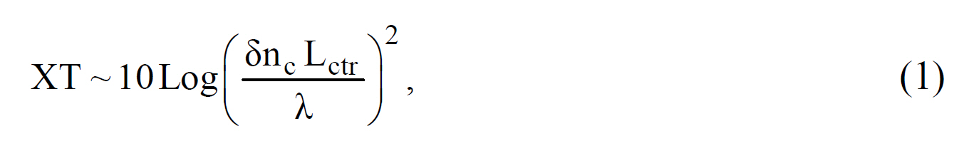
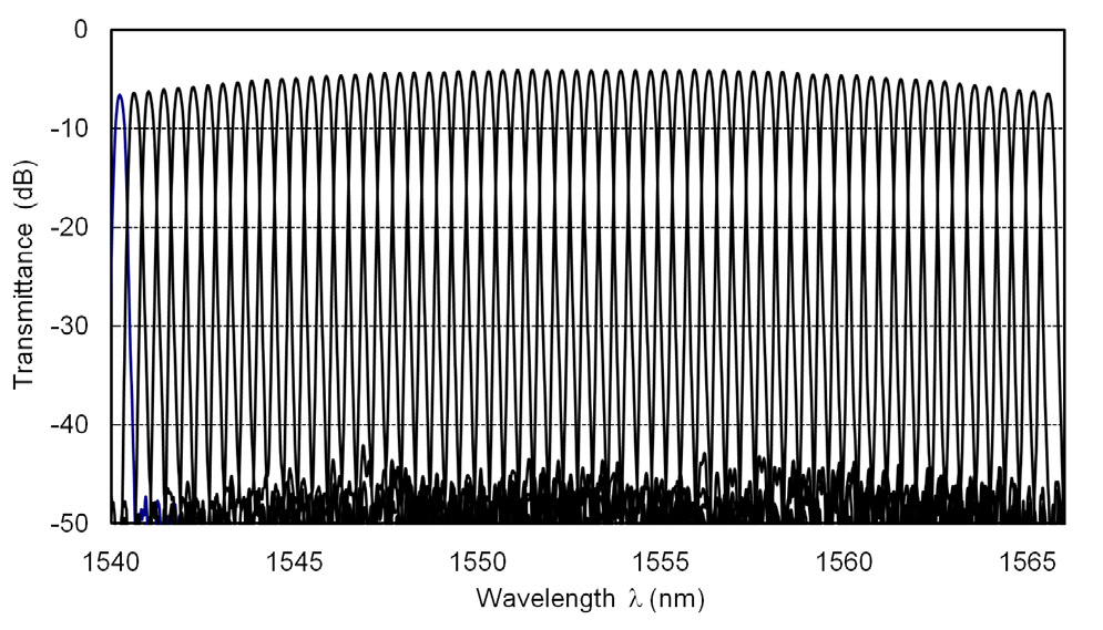
Effective-index fluctuation δnc in silica Planar Lightwave Circuits (PLCs) have been measured to be about δnc ~1×10?6 by using Fourier transform spectroscopy [5]. Good crosstalk characteristics are obtained in silica-based AWGs as shown in Fig. 1. The relation between the effective-index fluctuationδnc and crosstalk (XT) has been investigated theoretically and experimentally [6]. Based on the investigations, the empirical expression for the relation between δnc and XT has been obtained as
where Lctr and λ denote array waveguide length in the central region and the wavelength of light signal, respectively.Lctr of AWG in Fig. 1 is Lctr ~ 15 mm. Substituting
δnc ~ 1×10⁻⁶, Lctr ~ 15 mm, and λ = 1.55 ㎛ into Eq.(1), we obtain XT ~ -40 dB. Although Eq. (1) gives good agreement with the experimental results, the author believes that it should be proved analytically. Crosstalk of the planar Echelle gratings is obtained based on the similar investigations as
where ns and δζ denote the effective index in the slab region and the facet position fluctuation in the reflection mirrors. It is known from Eq. (2) that δζ should be about 5 nm in order to obtain -40 dB crosstalk in silica Echelle grating (ns ~ 1.5). Such a small δζ would be possible in the laboratory experiments [7]. However, the mask resolution for the commercial PLC products is normally about 25 nm~ 50 nm. This is the reason why commercial planar Echelle gratings could not achieve sufficient crosstalk value to be used in the current WDM systems.
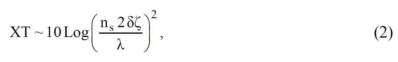
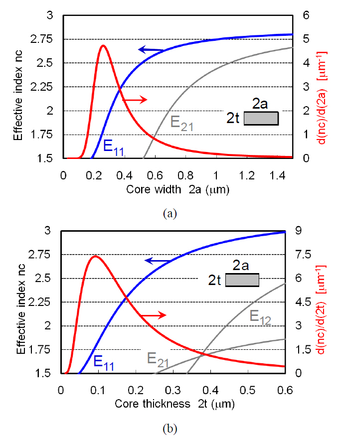
Effective-index fluctuation δnc in Si-wire waveguides has been evaluated from the measurements on the variation of resonant wavelength in the cascaded ring resonators [8]. Peak-to-peak resonance wavelength variation is 2δλ ~ 2.4 nm. Then, δnc is obtained as δnc=ncδλ/λ0~2×10-3 , where nc = 2.519 and λ0 = 1.55 ㎛. Effective-index fluctuationδnc in Si-wire waveguides can also be calculated by the vectorial finite element method [3]. Fig. 2(a) shows nc of Si-wire waveguide with thickness 2t = 0.22 ㎛ (blue) and its dependence on the core width 2a (red). dnc/d(2a)at the typical core width 2a = 0.5 ㎛ is 1.3 ㎛-1 = 1.3×10⁻³ nm-1.Fig. 2(b) shows nc of Si-wire waveguide with width 2a =0.5 ㎛ (blue) and its dependence on the core thickness 2t(red). dnc/d(2t) at the typical core thickness 2t = 0.22 ㎛ is 3.4 ㎛-1 = 3.4×10⁻³ nm-1.
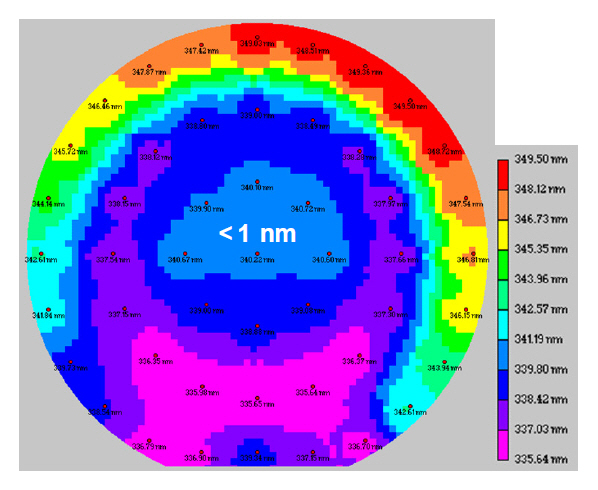
Core side-wall roughness of Si-wire waveguide is measured to be about σwidth ~ 2 nm [9]. Top silicon thickness uniformity of 6-inch SOI (silicon on insulator) wafer is measured to be about +/- 2 nm [10]. However, the photonic device occupies just ~1 mm square or less.
Then, the thickness fluctuation would be less than σthickness~ 1 nm as shown in the central region of Fig. 3 [6].Effective-index fluctuation δnc in Si-wire waveguide is then estimated to be δnc=[dnc/d(2a)]×σwidth~2.6×10-3 ,or δnc=[dnc/d(2t)]×σthickness ~3.4×10⁻³ , respectively. Both of the theoretical estimations for the effective-index fluctuation δnc agree well with the measured value. Effective index fluctuation δnc against core width variation can be reduced by enlarging core width in the straight regions. For example, dnc/d(2a) becomes to 0.35 ㎛-1 =3.5×10⁻⁴ nm-1 at 2a = 0.8 ㎛ [11] as shown in Fig. 2(a).
Si-rib waveguide structure allows us to obtain much smaller δnc as shown in Fig. 4, where core width W, core height H, and etch depth h are W = 0.5 ㎛, H = 0.3 ㎛,and h = 0.15 ㎛, respectively. dnc / dW at W = 0.5 ㎛ is 6.4×10⁻⁴ nm-1. However, the minimum bending radius becomes much larger compared to Si-wire waveguides and makes the device size larger. Therefore, Si-wire waveguide is still very attractive in making compact photonic devices.
Effective-index fluctuations of the order of δnc =3×10⁻⁴~ 2×10⁻³ determine the crosstalk values of the current Si-wire AWGs to be about -20 dB [11-13].
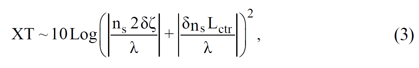
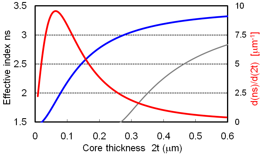
Echelle grating has been believed to be advantageous over AWG because only the facet position error causes crosstalk degradation. But, this is not true in Si Echelle grating since the effective-index fluctuation δns in the slab waveguide is substantially large as shown in Fig. 5. dns/d(2t) at the typical core thickness 2t = 0.22 ㎛ is 3.3×10⁻³ nm-1. Then, Eq. (2) for Si Echelle grating should be rewritten as
where Lctr denotes the total path length in the central region of the slab. Eq. (3) explains why large channel count(30 ch-3.2 nm spacing) Echelle grating has about -15 dB crosstalk, though small channel count (4 ch-20 nm spacing)one had about -30 dB crosstalk [14, 15]. The total path length Lctr in the large channel count Echelle grating is almost 5 times longer than that of small channel count one.Therefore, the second term in Eq. (3) becomes dominant in the large channel count Echelle grating.
In order to achieve good crosstalk characteristics (< -20 dB) in both Si-wire AWG and Echelle grating, (a) improvement in core width and thickness uniformity and/or(b) size reduction to make Lctr small are strongly required.
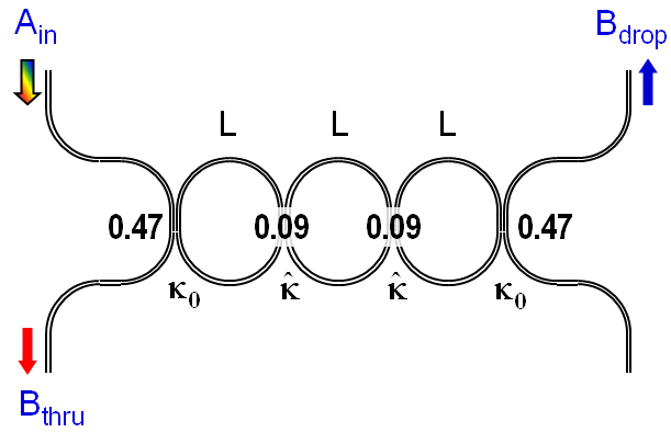
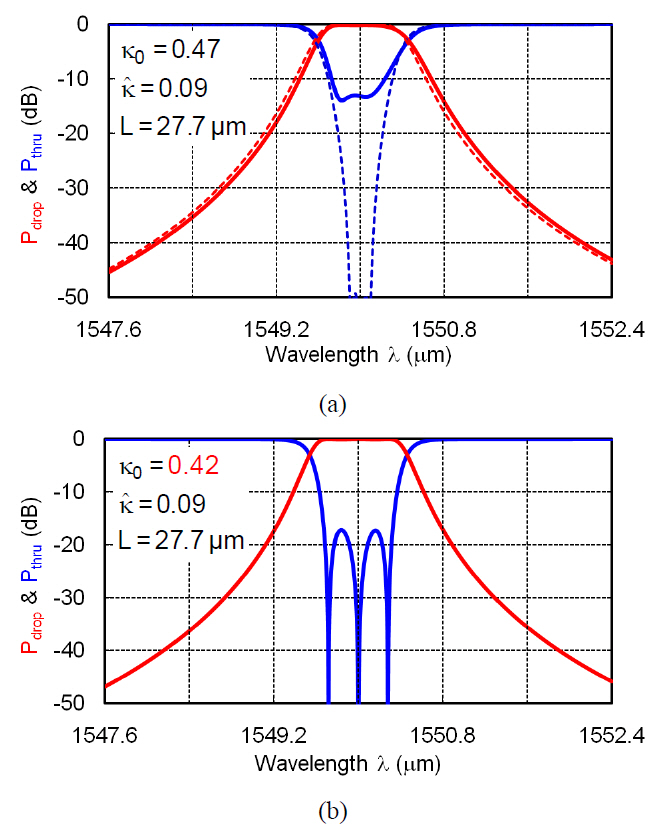
Cascaded ring resonators and lattice-form filters are also attractive candidates for filter applications in Si photonics.Fig. 6 shows coupled resonator optical waveguide (CROW)[1]. Kappa’s are amplitude coupling coefficients in the directional couplers. Ring perimeter L = 27.7 ㎛ for the ring diameter of 4.4 ㎛. Free spectral range (FSR)between the adjacent resonance order is about 2,600 GHz,which allows us to make 13 ch-200 GHz(1.6 nm) spacing WDM filter. FSR is inversely proportional to L.Therefore, ring resonator using other type of waveguide(such as silica PLC with bend radius of 5 mm) cannot obtain sufficiently wide FSR. Fig. 7(a) shows a filter response without effective index fluctuation (dotted lines)and with index fluctuation δnc = 5×10⁻⁴ only in the third ring (solid lines). It is shown that δnc less than 10-3 degrades crosstalk characteristics drastically. Fig. 7(b) is a filter response when κ0 is deviated from its ideal value 0.47 to 0.42. This amount of κ0 deviation can be caused by about +/- 13 nm gap width variation in the directional coupler.
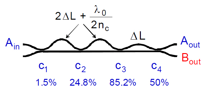
Fig. 8 shows schematic configuration of three-stage latticeform filter [2]. c1 to c4 are power coupling coefficients in the directional couplers. Channel spacing between the two
output ports is given by
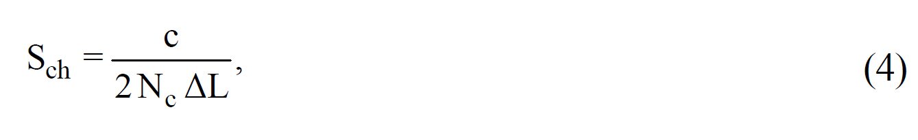
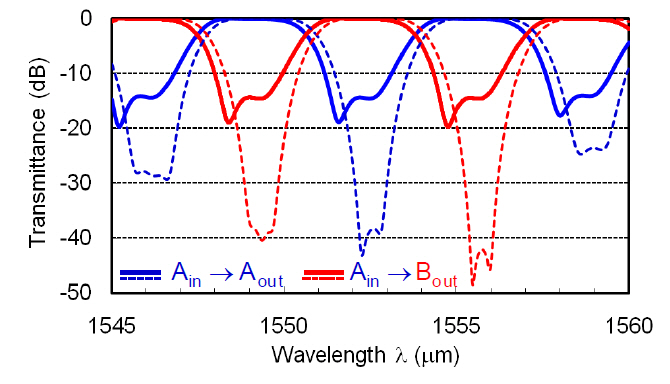
where ΔL, Nc and c are path length difference, group index (Nc=nc-λdnc/dλ) of the waveguide and light velocity. In the typical Si-wire waveguide, ΔL = 93 ㎛ gives the channel spacing Sch = 400 GHz. Fig. 9 shows a filter response without effective index fluctuation (dotted lines) and with random index fluctuation 'δnc' <5×10⁻⁴(solid lines). It is shown that δnc less than 10-3 degrades crosstalk characteristics drastically. It is also shown by other numerical simulation that when c2 is deviated from
its ideal value 24.8% to 17.8%, crosstalk becomes about-20 dB. This amount of c2 deviation can be caused by about +/- 20 nm gap width variation in the directional coupler. Experimentally, crosstalk level of about -10 dB has been obtained in Si-wire lattice-form filters [16].
Spatial heterodyne spectroscopy (SHS) is an interferometric Fourier-transform technique based on a modified Michelson interferometer with no moving parts and relying on analysis of stationary interference patterns [17]. In the bulk-optic SHS, the mirrors of the Michelson interferometer are replaced by diffraction gratings to offer scanning capability for two wavefronts. The SHS concept has been generalized into a waveguide Mach-Zehnder interferometer (MZI) array based on cosine fast Fourier transform (FFT) [18]. The path length difference in each asymmetrical MZI increases by ΔL, similar to AWG [3]. For any input wavelength, the entire output of a MZI array creates spatially oscillatory patterns, where the oscillation period is wavelength dependent due to the dispersive nature of the asymmetrical MZI.Each input wavelength has a unique fringe representation,which is the basis of the Fourier-transform relation between the input spectra and the output interferogram. Employing multiple input waveguides in the waveguide SHS is an important advantage over the existing AWG-type spectrometer,since it greatly increases the light capturing capability in proportion to the number of MZIs by using, for example,photonic lantern technology [19]. A photonic lantern is a device that efficiently converts light from a multimode fiber tip for light capturing to single-mode fibers connected to MZI input waveguides. The practical importance of the Fourier-transform spectrometer is the ability to correct for interferometer defects (phase errors) in data processing stage. The first waveguide SHS have been fabricated in silicon-on-insulator rib waveguides using stacks of multiple MZIs [20]. However, a measurement result on the spectrum has not been reported so far to our knowledge.
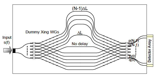
We reported a novel planar waveguide SHS configuration with an interleaved MZI array [21]. The interleaved configuration allows us to put 2~3 times more MZIs than the simple stacking layout when we compare two layout methods for the same spectrometer parameters. We made an array of 32 MZIs in silica-based PLC. The path length difference increment was ΔL = 162 ㎛, which resulted in 20 GHz resolution at the 1.55 ㎛ region. Phase errors in the asymmetrical MZIs were measured by the thermo-optic phase scanning method [22]. The spectrum of the light source was successfully retrieved by correcting the MZI output data with the phase error values.
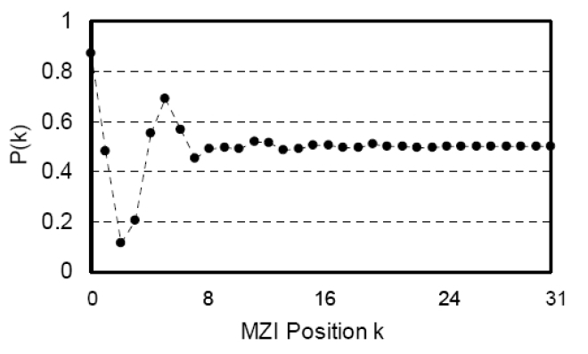
Figure 10 shows the configuration of the novel waveguide SHS with the interleaved MZI array. The total number of MZIs is N = 32. The waveguide core size is 4.5㎛× 4.5 ㎛ with 1.5% refractive-index difference.The minimum bend radius is 2 mm. White boxes indicate 3 dB couplers consisting of either directional couplers or multimode interference couplers. The input and output waveguide separations at the chip ends are 15 and 50 ㎛,respectively. Waveguide arms in the MZI are intentionally inclined to both sides so that the waveguides intersect by more than 45º with each other. It is known that the excess loss of the waveguide crossing can be reduced as low as~ 0.02 dB/intersection when crossing angle is larger than 45º [23]. Dummy crossing waveguides are placed to make the total number of waveguide crossing equal for all MZIs. The chip size, including input and output fan-out regions, is 43mm× 25 mm . We measured both cross-port and through-port outputs p (k ) and q(k) in the k-th (k = 0~ N-1) MZI so that the spatial nonuniformity of the input light distribution can be corrected. The output power of each port was measured by shifting the single-mode fiber in the current preliminary experiments. Fiber-to-fiber loss of MZIs are measured to be 4.2 ~ 5.4 dB.
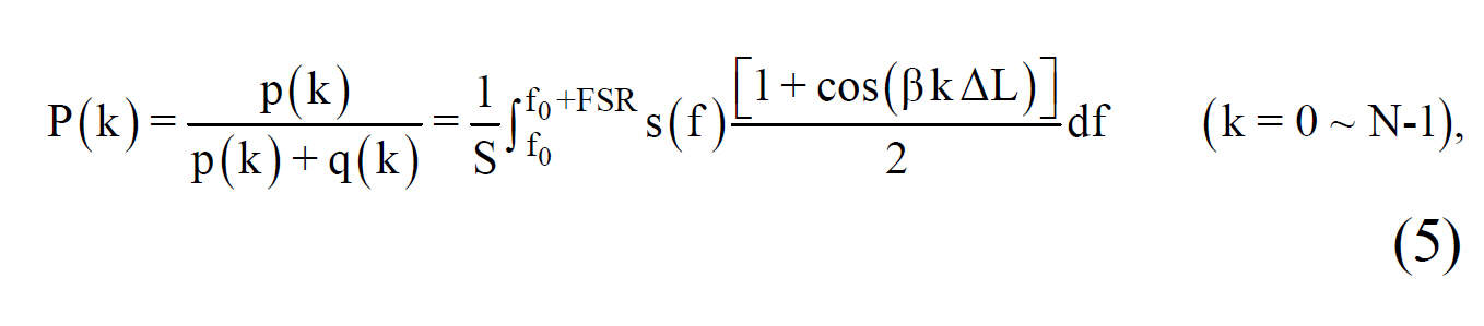
The operational principle of a SHS spectrometer based on the MZI array has been elaborated in [18]. For a signal s ( f ) passing through the k-th MZI, a normalized cross-port output is given by assuming negligible waveguide loss as
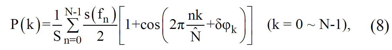
where β is a propagation constant, FSR is a free spectral range determined by ΔL, and S = ∫f0 f0+ FSR s( f )df . f0 is denoted as the Littrow frequency at which phase delays in different MZIs become integer multiples of 2π(β ( f0 )ΔL= 2mπ ). Since MZI response repeats periodically with FSR, one needs to block the unnecessary spectral range by a bandpass filter. Based on the discrete cosine Fourier transform, the input spectrum s( fn ) ( fn =f 0 + n ? FSR/□, where □=2N=64) can be calculated from the measured output power P(k) as
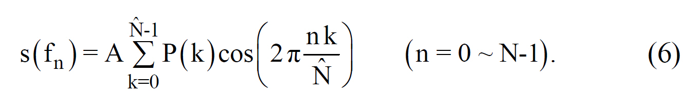
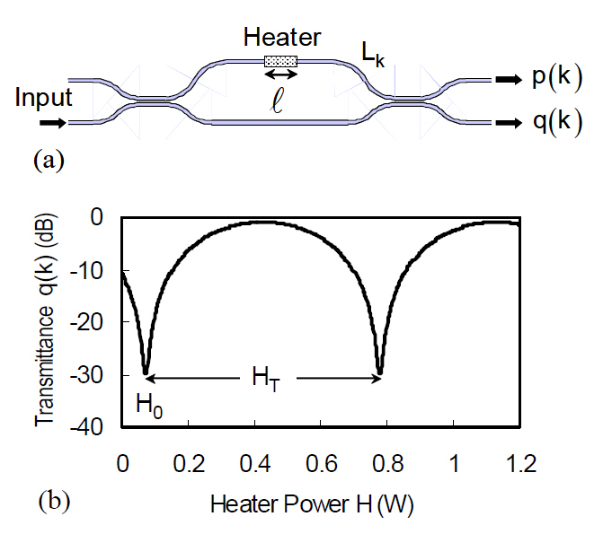
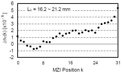
In the above equation, A is a constant and P(k) for n=N~ □ ?1 is assumed to be P(□ ?k). Although FSR was sampled with N points in [18], we sample it with 2N points in order to correctly represent the MZI outputs. Because MZI responses for the signal in the upper half of FSR, s( fn ) (n=N~□ ?1), have identical spatial fringe representation to those of the signal in the lower half, only the lower half of the signal spectrum can be measured. Resolution of the spectrometer is given by δ f=c/(□ncΔL)=20 GHz. Phase errors caused by effectiveindex fluctuations in the MZI array deteriorate the accuracy in the retrieved signal by Eq. (6).Phase error δφk in the k-th MZI is expressed as δφk= (2π/λ0 )δnc(k)Lk ,where δnc(k) and Lk denote effective-index fluctuation and MZI arm length, as shown in Fig. 11(a). A heater with length l was placed from outside of the chip on either one of the MZI arms to measure δφk. The through-port transmittance q(k)under the thermo-optic effect is given by
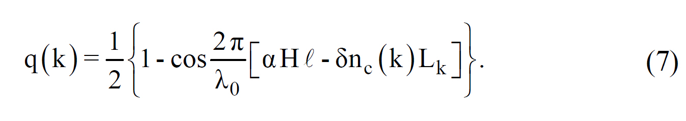
Here, H is a heater power applied to the phase shifter, α is a coefficient of thermo-optic refractive-index change per unit heater power and λ0=c/ f0. Figure 11(b) shows an example of the thermo-optic phase scanning measurement.The first extinction point indicated by H0 corresponds to the point at which the phase error is compensated for. The power between two adjacent extinction points HT corresponds to an optical path length change with λ0. δφk is then given by δφk=2π ?H0/HT. Effective-index fluctuation is obtained as δnc(k) =(δφk/Lk)λ0/2π . Measured
δnc (k) in the MZI array is shown in Fig. 12.
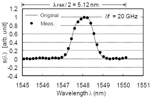
A major advantage of the waveguide SHS based on Fourier-transform spectroscopy is that the interferometer defects due to effective-index fluctuations can be corrected in data processing stage. On the contrary, physical refractiveindex correction has been required for AWGs after the phase error measurement [24]. A known signal spectrum was coupled into the waveguide SHS. The normalized cross-port output power distribution P(k) and the retrieved signal spectrum s(λn)(λn=c/ fn) by the cosine FFT are shown in Figs. 13 and 14, respectively. The Littrow wavelength λ0 was determined by measuring the normalized cross-port output at the second MZI P(k =1). P(1) rapidly oscillates with respect to the wavelength change. But, it reaches to stationary and the maximum value at λmax=λ0[1+δφ1/(2πm)]~λ0. λ0 was measured to be 1550.1 nm. Solid curve in Fig. 14 is the original signal spectrum measured by a bulk spectrometer. The Hanning
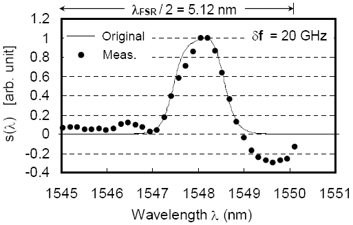
window was multiplied to P(k) so as to reduce oscillatory features in the retrieved spectrum. The FSR in terms of wavelength is given by λFSR = λ0 /m = 10.24 nm. Signals in the range of λ = 1539.9 ~ 1545.04 nm are not shown in Fig. 14 since they are mirrored replica of the spectrum in λ = 1545.2 ~ 1550.1 nm. Deviation of the measured spectrum from the original one is mainly due to the phase error δφ'ks since they cannot be directly included in the cosine FFT analysis. The horizontal axis in Fig. 13 is understood to be the optical path length difference divided by ncΔL. Then, the measured MZI output should be located at k+δncLk /ncΔL instead of the ideal position, k . The correction can be done by using the measured data and the Lagrange interpolation to replace the unevenly spaced interferogram points by the evenly spaced ones[25]. Fourier-transform algorithms can then be applied to the evenly spaced interferogram points. For a large number of data points, as in bulk-optic Fourier-transform spectroscopy,a FFT-based procedure is a prerequisite. However,for a small number of N, the discretized form of Eq. (1), including phase errors,
can be solved by N×N simultaneous equations. A signal spectrum corrected with the above procedure is shown in Fig. 15. The main part of the spectrum is accurately retrieved. Some oscillatory features in the peripheral spectral regions may be caused by the imperfection of the 3 dB couplers and differential attenuation in longer asymmetrical MZIs. Correction of these imperfections will be reported in the future.
Four kinds of silicon photonics WDM filters have been investigated in detail. It is made clear that (a) improvement in core width and thickness uniformity and (b) size reduction to make the device size small are strongly required in order to achieve good crosstalk characteristics(< -20 dB).
We have demonstrated a novel planar waveguide spectrometer implemented in silica PLC. The signal spectrum was successfully retrieved by correcting the MZI output data with the phase error values. Miniature spectrometers will be important for daily health care and environmental sensing applications since they are compact in size and potentially very low cost (disposable).