검색 전체 메뉴
PDF
맨 위로
OA 학술지
Retardation Free In-plane Switching Liquid Crystal Display with High Speed and Wide-view Angle
  • 비영리 CC BY-NC
  • 비영리 CC BY-NC
ABSTRACT
Retardation Free In-plane Switching Liquid Crystal Display with High Speed and Wide-view Angle
KEYWORD
In-plane switching , Retardation free , Wide viewing angle , Fast response , Low cell gap , (120.2040) Displays , (160.3710) Liquid crystals , (230.2090) Electro-optical devices
  • I. INTRODUCTION

    As many people are more familiar with the widespread information-oriented society, further progress toward highdisplay quality is needed to use the display devices as informational interfaces. In particular, the in-plane switching (IPS)LC mode [1] and the vertical alignment LC mode [2, 3] are representative LCD modes for the required electro-optical characteristics in the current display devices, such as a wide-angle viewing, color shift and so on. In terms of the response times, however, all advanced LCD modes, including IPS LC cells, do not show sufficient high-speed properties for video rate images, despite the development of technologies that improve the response time. In particular, display devices are recently being required for application to the 3D moving pictures that need fast-response LCDs in order to minimize the cross-talk [4-6], so that development of high speed and high quality LCDs is needed.

    In general, the response time of an IPS LC cell is defined by the summation of the rising time and falling time when voltage is applied. These variables can be calculated as follows [7]:
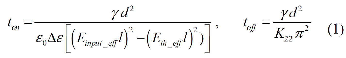
    image

    Where, ton and toffare rising and falling times; ε0, Δε, γ,and k22 represent the permittivity in free space, dielectric anisotropy, viscosity and twist elastic constant of the LC material, respectively; d is the cell gap of the LC cell; and l represents the distance between the electrodes. Einput_eff and Eth_eff represent the effective input electric field and the effective threshold electric field.

    From the Eq. (1), we can see that the response time can be improved by controlling the parameters of the LC cells.First, there can be an improvement of the LC material that permits small viscosity γ, high dielectric constant Δε and high elastic constant k22. However, current LC materials for LC cells are almost optimized for fast-response times,so it is hard to improve these parameters effectively without any electro-optical characteristic deficiency. Second, to get faster response times involves reducing the cell gaps of the LC cells. In order to achieve a bright state in a conventional LC configuration, light passing through the LC cell in front of the output polarizer should have half-wave retardation.Therefore, the refractive anisotropy (Δn) of the LC materials should be high enough to keep the cell gap (d) small. In general, a practical approach to getting the high anisotropy of LC materials can reduce the optimized value of the viscosity γ of the LC materials, so that the response time cannot be decreased effectively.

    In this paper, we propose a configuration of a retardation free (RF) IPS LC cell for a fast response time by adding an A-plate. This optical configuration is not affected by the retardation of the LC cell if it has more than quarterwave retardation. Therefore, we can reduce the cell gap d as the process permits for a faster response time without any changes in the LC materials. We calculated the electrooptical characteristics of the RF LC configuration in order to compare the calculated results to the conventional IPS LC cells. In addition, we also propose an optical configuration of the RF IPS LCD with wide viewing angle. The wide-view IPS LCD, therefore, can provide the fast response time and the wide viewing angle simultaneously.

    II. OPTICAL RESPONSE OF THE RF IPS LC CELL

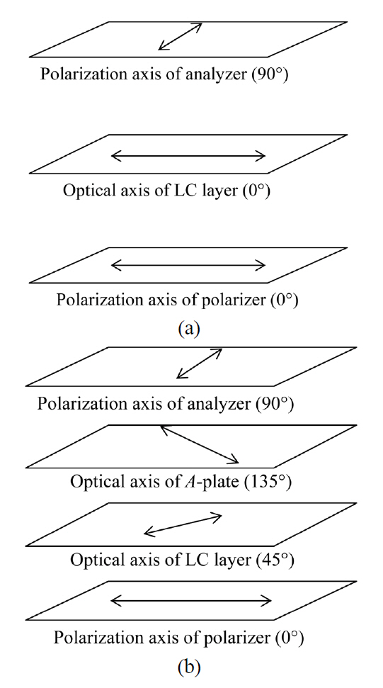
    The basic optical configuration of a conventional IPS LC cell consists of two crossed polarizers and an LC cell with half-wave retardation as shown in Fig. 1 (a). The initial state of the LC cell has an optical axis parallel to the input polarizer. Then, the light passing through the input polarizer cannot experience optical retardation, even if it passes through the LC cell, because the polarization axis of the input polarizer and the optical axis of the LC cell coincide. Therefore, the polarization of the light in front of the output polarizer stays perpendicular to the polarization axis of the polarizer, so that we can achieve a dark state.For a bright state, the effective optical axis of the LC layer should rotate to 45° by the applied voltage and the LC layer should show half-wave retardation. Then, the light passing through the input polarizer experiences half-wave retardation, so that the polarization of the light passing through the LC layer rotates 90° in front of the output polarizer,which parallels the polarization axis of the output polarizer.Thus, we can achieve a bright state. In this case, we can make a half-wave LC cell with an excellent bright state that

    depends strongly on the retardation Δnd of the LC cell in the optical design.

    Compared with a conventional LC cell, the RF LC cell is independent on the retardation of the LC layer, in principle,if it has more than quarter-wave retardation. Figure 1 (b)shows the basic optical configuration of the RF IPS LC cell that is sequentially stacked by an A-plate with an LC layer between the two crossed polarizers. The A-plate in the cell should have exactly the same retardation as the LC layer, and its optical axis is exactly crossed to the optical axis of the LC layer. In the no-voltage state, the light passing through the input polarizer will pass through the LC layer, so that the polarization of the light passing through the LC layer will be changed to the other polarization state. However, the polarization state of the light will return to the polarization axis of the input polarizer by passing through the A-plate because the A-plate has exactly the same retardation and the crossed optical axis as the LC layer. This can make a perfect dark state. The bright state of the RF IPS LC cell can be obtained by rotating the optical axis of the LC layer by applying the voltage, so that the summation of the effective Δnd of the LC layer and the retardation of the A-plate will be halfwave retardation. Basically retardation in the bright state for half-wave retardation can be provided in part by the A-plate, so that we can reduce the effective Δnd of the LC layer by even quarter-wave retardation. Therefore, we can also reduce the cell gap d of the LC layer without changing the LC material. This can induce a fast response time for the IPS LC cell compared with the conventional IPS LC mode.

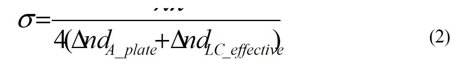
    The rotational angle σ of the effective optical axis of the LC layer for the bright state depends on the retardation of the used Δnd of the LC layer and the A-plate, which means that the rotational angle of the effective optical axis of the LC layer should be determined so the total retardation of the effective Δnd of the LC layer (ΔndLC_effective) and the A-plate (ΔndA_plate) as to be λ/2 for the excellent bright state. The range of the rotational angle of the effective optical axis of the LC layer can be π/4 to π/2. At π/4 rotation, the (ΔndLC_effective) is 0 because the optical axis of the LC layer is coincident or perpendicular to the polarization axis of the polarizer. In contrast, at π/2 rotation, the (ΔndLC_effective) is maximized because the optical axis of the LC layer makes π/4 as for the polarization axis of the polarizer. Therefore, if the Δnd of the LC layer and the A-plate are quarter-wave, which means ΔndLC_effective +ΔndA_plate = λ/2, then  should be π/2. And if the Δnd of the LC layer and the A-plate are half-wave, which means ΔndLC_effective +ΔndA_plate = λ, then  should be π/4. At middle range of the ΔndLC_effective +ΔndA_plate between λ/2 to λ, we can assume that the  should be linearly changed between π/4 to π/2. From this, we can simply calculate the equation (ΔndLC_effective +ΔndA_plate) σ = (λπ)/4 for determining the σ. As a result, the effective rotation angle of the LC director can be described as below:

    image

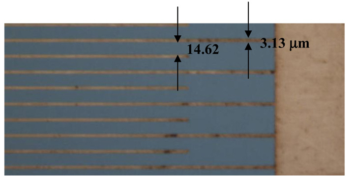
    To compare the optical response of the RF IPS cell with conventional LCD, we started to investigate the appropriate driving voltage of the conventional IPS cell. For this calculation, we applied a single domain IPS LC cell that has a 3.13 ㎛ electrode width and 14.62 ㎛ of space between the electrodes. Figure 2 (a) shows the calculated optical response of the conventional IPS cell as a function of the voltage applied for 100 ms to the cell. The used LC material is ML-0249, which was made by Merck, (γ =74 mPa sec , ε = 3.6, ε// = 12, k11 = 12.8 pN, k22 = 5.8 pN, k33 = 12.5 pN, ne = 1.58101, no = 1.48167). Cell gap of the LC cell is 3.4 ㎛. In Fig. 2, the optical response of the conventional IPS cell can be optimized at 8V. In the voltage range over 9V, we observed the overshoot at the edge of the optical response due to the higher voltage.And, the transmittance of the optical response became lower at 8V because the effective optical retardation of the LC cell deviates from half-wave retardation. Figure 2 (b) shows the experimental verification of the calculation. The calculation was performed by software TECHWIZ LCD made by SANAYI system. We can observe the overshoot at over 8.5V in the conventional IPS LC cell. Then, we compared the optical response of the RF IPS LC cell with a conventional IPS LC cell at 8V.

    As described, the RF IPS LC cell uses the optimized LC material which is used in a conventional LCD (ML-0249),because the A-plate can compensate for the LC layer completely during the dark state. To compare the optical response, we calculated the optical response of the RF optical

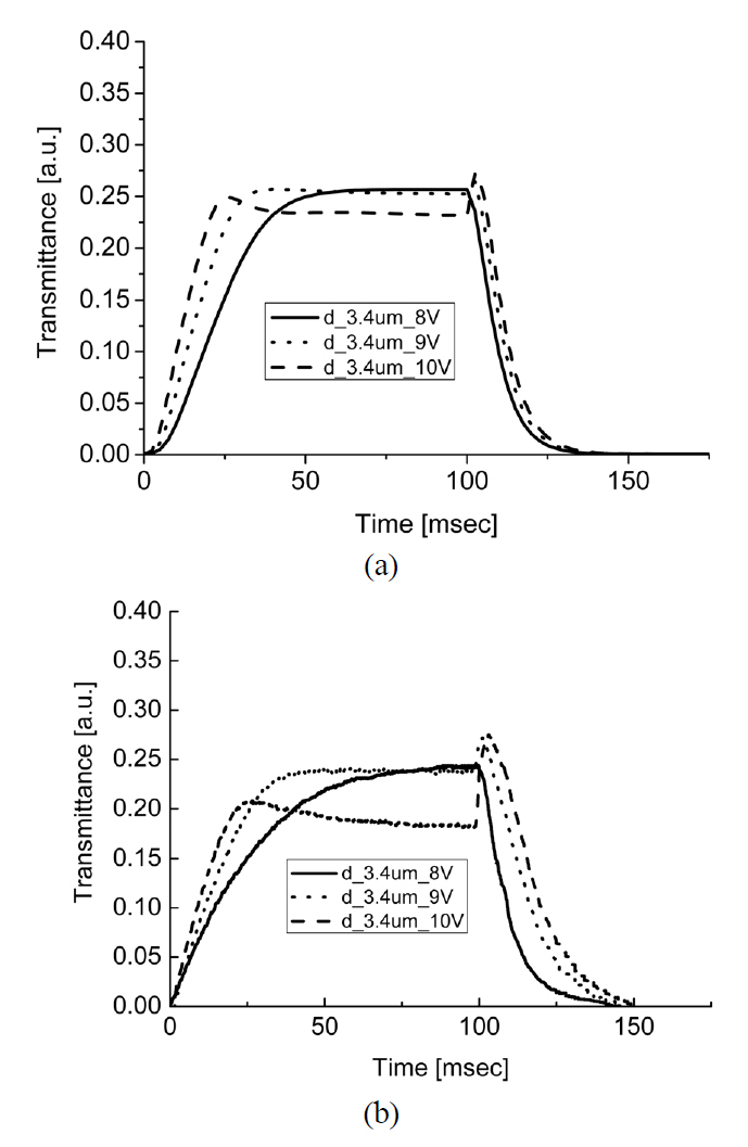
    configuration with quarter-wave retardation (cell gap d =1.41 ㎛) and 0.3612-wave retardation (cell gap d = 2 ㎛)to the conventional cell. For the bright state, we can calculate the rotation angle of the effective optical axis of the LC layer as σ = 90° for the quarter-wave retardation cell and σ = 76.5° for the 0.3612-wave retardation cell. Figure 3 shows the calculated optical response of the IPS LC cells. The solid line, dotted line and dashed line represent the optical response of the conventional IPS cell,0.3612-wave retardation cell, and quarter-wave retardation cell. The optical response of the 0.3612-wave retardation cell was optimized at 12.8V. In particular, the quarter-wave LC cell showed lower transmittance compared with the other IPS modes, even after we increased the voltage to 17V, because quarter-wave LC cells should make all LC directors rotate 90° in order to make optimized bright state.However, surface anchoring energy of the cell can disturb the perfect 90° rotation of the LC director, so that we can hardly achieve the good transmittance even if we increase the voltage. Figure 3 also shows a summarized comparison of the calculated optical properties of the RF IPS LC cells compared with the conventional LC cells. In Fig. 3, we can see that the response time of the RF IPS LC cell was

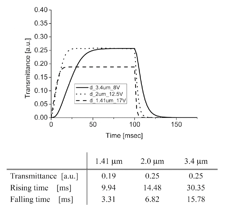
    reduced significantly because of the low cell gap and the optimized LC materials. Especially, we can look into the falling time, which is the most important time because it is uncontrollable with applied voltage, but it depends on the LC materials’ properties, and it can be decreased compared with the conventional IPS LC cell. In contrast,we can also observe that the RF IPS LC cell requires a higher voltage compared with the conventional IPS cell because of a low cell gap. In spite of this deficit, we can expect the fast response IPS LC cell without significant voltage loss by using the RF optical configuration. For example, the 0.3612-wave retardation cell, which requires more than 4V or 5V compared to the conventional cell, can reduce falling time over 57% compared with the conventional IPS LC cell without a loss of the transmittance. This may be not suitable for mobile application, but is suitable for high speed LCD application such as the 3D TV.

    To verify the improvement of the optical response to the RF IPS LC cell, we made an experiment to measure the optical properties with the same conditions and calculations. Figure 4 shows the microphotograph of a single domain IPS LC cell. The width of the electrode and the spatial interval between the electrodes are 3.13 ㎛ and 14.62 ㎛,respectively, which are the same as for the calculation condition. The alignment layer is spin-coated. We set uniformly cell gap by using a ball spacer. Also, the A-plate which has the same retardation as the LC layer and its optical axis is crossed to the optical axis of the LC layer was attached on the LC cell.

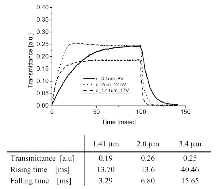
    Figure 5 compares the measured optical response of the RF IPS LC cells with the conventional IPC LC cells. In the figure, we could confirm that the RF IPS LC cell can reduce the response time due to a low cell gap without any degradation of the transmittance of the bright state.Especially, the low cell gap of the RF IPS LC cell can provide the very fast falling time in the response time.

    III. AN OPTICAL CONFIGURATION OF THE RF IPS LC CELL FOR WIDE VIEWING ANGLE

    In general, degradation of the optical viewing angle of the LC cell in oblique incidence can have several reasons such as the change of the optical axis and the retardation of the optical retarder that is used, the change of the polarization axis of the polarizer in oblique incidence [7, 8]. In terms of the polarizer and the A-plate, if we apply the very small birefringence approximation (ne ? no), the deviation of the azimuth angle δ from δo can be described as below [7]:

    image

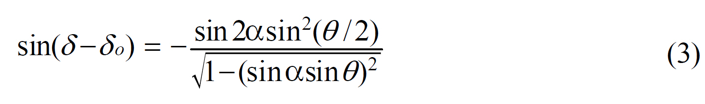
    where α is the azimuth angle of the axis of the polarizer,and θ is the polar angle of the incident light in the LC layer. δo represents the angle between the polarization axis of the polarizer and the x-axis at normal direction. The optical axes of the A-plate and the LC layer have a same deviation angle δ with polarization axis of the polarizer in oblique incidence. Moreover, the retardations of the A-plate and the LC layer are changed as functions of the polar and the azimuth angle of the oblique incident light. The effective retardation of the A-plate and the LC layer can be expressed as follows [9, 10],

    image

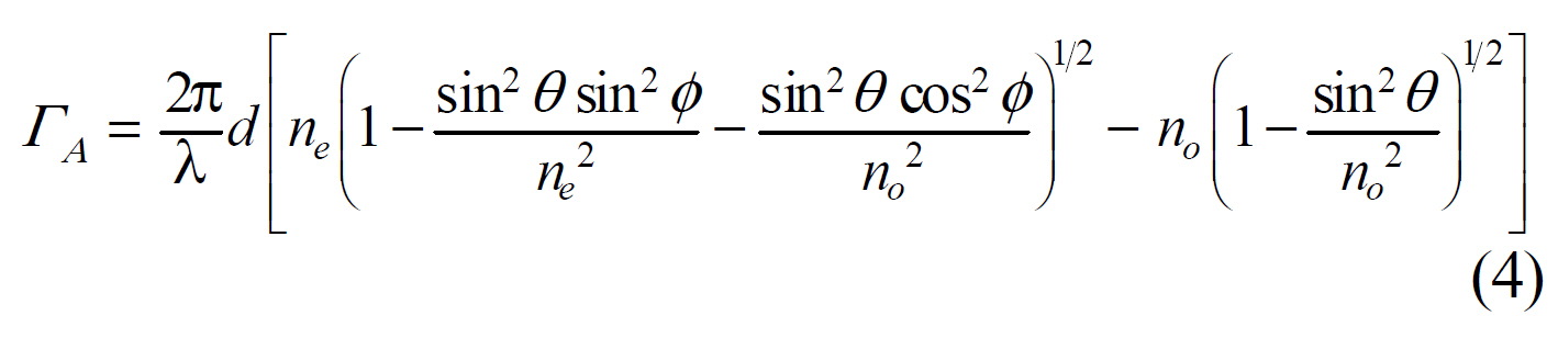
    where ΓA represents the phase retardation of the A-plate and the LC layer at the oblique incidence, respectively. φ and d are the azimuth angle of the incident angle and the thickness of the film or the LC layer, respectively. ne and no are the refractive indices of the birefringence layer.

    In spite of the optical merits of the RF IPS LC cell, we can predict the narrower optical viewing angle compared to the conventional IPS LC cell because all principle axes and the Δnd of the used optical components including polarizer, the A-plate and the LC layer can be changed in all directions.

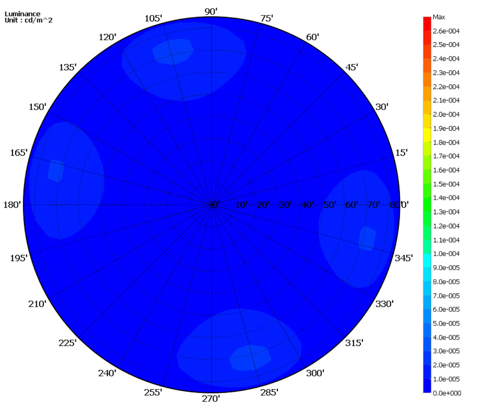
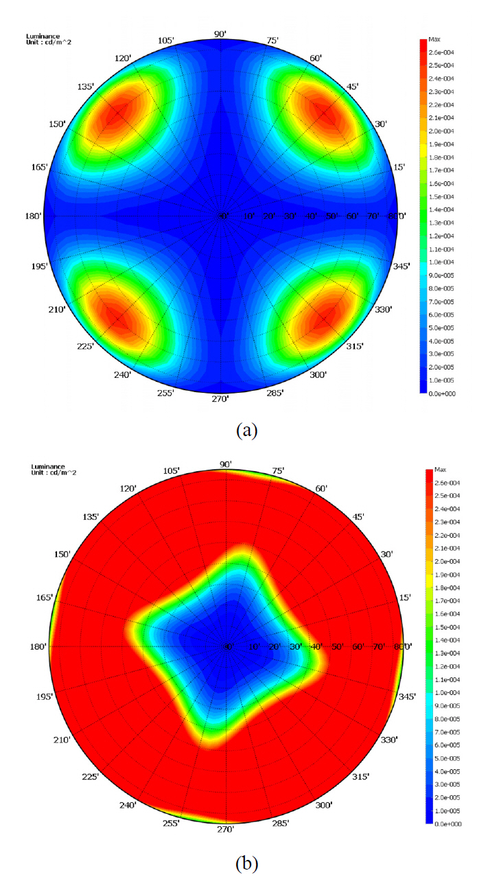
    Figure 6 shows the light luminance of the conventional IPS LC cell and the RF IPS LC cell in the dark state.Retardations of the LC material used and of the A-plate are 0.3612 λ. In the Fig. 6, we can easily observe the serious optical leakage of the RF IPS LC cell in all directions in the dark state even compared to the conventional IPS LC cell.

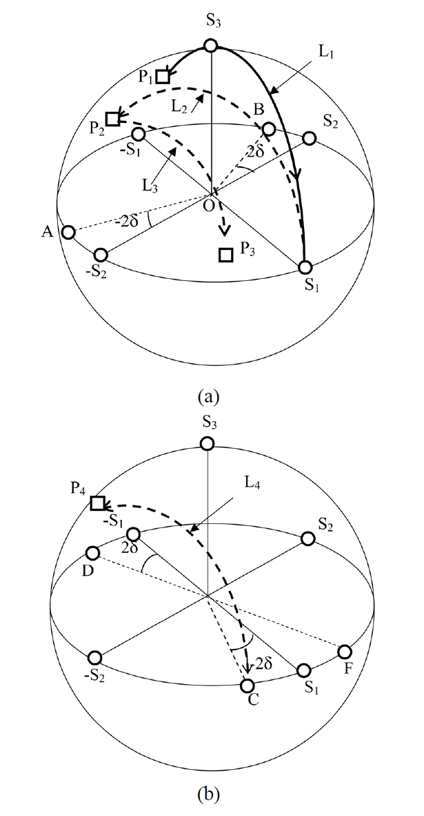
    Figure 7 (a) shows why the light leakage of the RF IPS LC cell happens in the horizontal and vertical directions on the Poincare sphere. In the normal direction, the positions of the polarizer and the LC layer lie on S1 and S2, which determine the linear horizontal polarization and the 45° linear polarization, respectively. And the positions of the polarization axis of the analyzer and optical axis of the A-plate are ?S1 and ?S2, which are the exact opposite positions of the polarization axis of the polarizer and the optical axis of the LC layer, respectively. The polarization of the light passed through the polarizer lies on the position S1. And it will rotate to the position P1 as much as the retardation of the LC layer through line path L1 with a centered position S2. The polarization passing through the A-plate will go back to the start position S1 through path L1 again because the retardation of the A-plate is the same as the LC layer and the position of the optical axis of the A-plate is ?S2, which is the exact opposite position of the LC layer, so that we can get an excellent dark state.In oblique incidence, however, the optical axis of the LC layer and the A-plate will deviate to positions B and A from S2 and ?S2 with deviation angle δ as shown in Fig.7 (a). As a result, the rotation paths by the LC layer and the A-plate can be changed to L2 and L3 from L1 because the centered positions for rotating the polarization of the light passing through the LC layer and the A-plate are changed to the position C and A from S2 and ? S2, respectively.Therefore, the polarization of the light passing through the cell will move to the position P2 by the LC layer and finally it will move to the position P3, which is deviated from S1, in front of the analyzer so that the light leakage happens in the oblique incidence.

    As for the diagonal direction, we can predict more serious light leakage. Figure 7 (b) shows the light leakage of the cell in the diagonal direction on the Poincare sphere. In the diagonal direction, the polarization axis of the polarizer and the analyzer are changed with deviation angle δ, which are positions C and D as shown in Fig. 7 (b). The positions of the optical axis of the LC layer and the A-plate are never changed in oblique diagonal directions. Therefore,the positions of the optical axis of the LC layer and the A-plate are S1 and ?S1 on the Poincare sphere. As a result,the polarization of the light passed through the LC layer is rotated to P4 along the path L4 with a centered position S2

    and it will rotate back to the position C along the path L4 again by the A-plate. The position C is so far from the opposite position of the analyzer F that serious light leakage can occur.

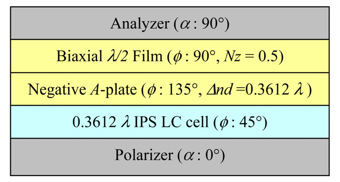
    In order to enhance the optical viewing angle of the RF IPS LC cell in the dark state, we propose a wide-view RF IPS LC cell that can protect the light leakage in oblique directions as shown the Fig. 8. We apply a negative A-plate instead of the positive A-plate for reducing the light leakage in the vertical and horizontal directions. In addition,we also apply a biaxial half-wave film whose optical axis is exactly the same as the polarization axis of the paired polarizer for decreasing the light leakage in the diagonal direction.

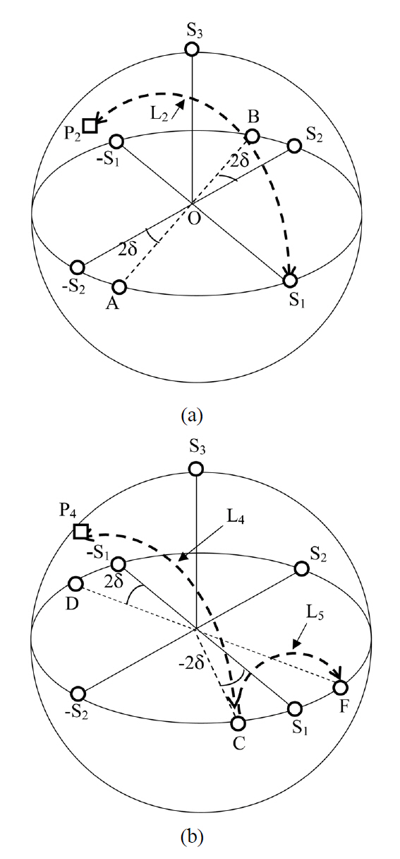
    In the horizontal and vertical directions, we observed the change of the optical axis and the Δnd of the LC layer and the A-plate in oblique incidence as shown in Fig. 7.(a). However, the negative A-plate in Fig. 8 can compensate the deviated polarization of the light passed through the LC layer by the oblique incident in horizontal and vertical

    direction exactly as shown in Fig. 9 (a). The deviation angle of the optical axis of the negative A-plate is 2δ on the Poincare sphere, which is exact opponent position of the optical axis of the LC layer in oblique direction as shown in Fig. 9 (a). Therefore, the polarization of the light can be returned to the start position S1 by passing through

    the negative A-plate even if the light passes through the LC layer with oblique angle.

    In the diagonal direction, the biaxial λ/2 plate can move the deviated polarization of the light passed through the LC layer to the opponent position F against the position of the polarization axis of the analyzer on the Poincare sphere as shown in Fig. 9 (b). As we described in Fig. 7(b), the polarization position of the light passed through the LC layer and the negative A-plate is on the position C.For oblique diagonal incidence, positions C and F deviated with -2δ and 2δ from the position S1 on the Poincare sphere.Therefore, we can move the polarization of the light on the position C to the position F along the path L5 by passing through the λ/2 plate as shown in Fig. 9 (b). The biaxial film with 0.5 of the value Nz has almost constant value of the retardation and the optical axis in arbitrary oblique incident angle [8]. Therefore, the biaxal λ/2 plate(Nz = 0.5) will successfully move the polarization of the light passing through the LC layer and the negative A-plate to the goal position F on the Poincare sphere, so that it can effectively block the light leakage in the diagonal direction for dark state.

    Figure 10 shows the calculated iso-luminance of the wide-view RF IPS LCD in the dark state. Iso-luminance in the Fig. 10 shows the excellent dark state compared to the conventional IPS LC cell.

    IV. CONCLUSION

    We proposed an IPS LC cell, that is free of retardation,by using an applied A-plate which has exactly the same retardation as the LC layer. In contrast to the conventional IPS LCD, the optimized bright state of the RF LC cell can be achieved by the rotation angle of the LC layer. This configuration could reduce the cell gap of the LC layer by quarter-wave retardation without any changes to the optimized LC materials, so that we could expect the fast response time by reducing the cell gap of the LC layer. We may make use of the reactive mesogen (RM) technology instead of the A-plate in order to complete the RF IPS LC cell because the RM is more suitable for compensating for the dispersion of the optical anisotropy of the LC layer than the A-plate. We also completed a wide viewing property of the RF IPS LCD by applying a negative A-plate and a biaxial λ/2 plate. We believe that this configuration can be appropriate to the requirements of the current display device such as the fast response and the wide viewing angle. Therefore, the RF IPS LC cell can be applied to the display devices such as 3D displays that require a very fast response time and excellent optical properties.

참고문헌
  • 1. Oh-e M, Kondo K 1995 Electro-optical characteristics and switching behavior of the in-plane switching mode [Appl.Phys. Lett.] Vol.67 P.3895-3897 google cross ref
  • 2. Takeda A, Kataoka S, Sasaki T, Chida H, Tsuda H, Ohmuro K, Koike Y, Sasabayashi T, Okamoto K “A superhigh-image-quality multi-domain vertical alignment LCD bynew rubbing-less technology” P.1077-1080 google
  • 3. Kim K. H, Lee K. H, Park S. B, Song J. K, Kim S. N, Souk J. H “Domain divided vertical alignment modewith optimized fringe field effect” P.383-386 google
  • 4. Seo D. S, Lee J. H 1999 Wide viewing angle and fast response time characteristics of nematic liquid crystal using novel vertical-alignment-1/4π cell mode on homeotropic alignment layer [Jpn. J. Appl. Phys.] Vol.38 P.1432-1434 google cross ref
  • 5. Cho I. Y, Kim S. M, Hwang S. J, Kim W. I, Kim M. Y, Son J. H, Ryu J. J, Kim K. H, Lee S. H “Newvertical alignment liquid crystal device with fast response time and small color shift” P.246-248 google
  • 6. Hong H. K, Lim M. J 2009 Response time characteristics of optical shutter of vertical alignment liquid crystal cell for obliquely incident light [Liquid Crystals] Vol.36 P.109-113 google cross ref
  • 7. Yeh P, Gu C 1999 Optics of Liquid Crystal Displays google
  • 8. Saitoh Y, Kimura S, Kusafuka K, Shimizu H 1998 Optimum film compensation of viewing angle of contrast in in-planeswitching-mode liquid crystal display [Jpn. J. Appl. Phys.] Vol.37 P.4822-4828 google cross ref
  • 9. Zhu X, Ge Z, Wu S.-T 2006 Analytical solution for uniaxialfilm-compensated wide-view liquid crystal display [J. Dis. Technol.] Vol.2 P.2-20 google cross ref
  • 10. Yang D.-K, Wu S.-T 2006 Fundamentals of Liquid Crystal Devices google
OAK XML 통계
이미지 / 테이블
  • [ FIG. 1. ]  Comparison of the initial optical configuration of theconventional IPS LC cell and the RF IPS LC cell: (a)conventional cell (b) RF cell.
    Comparison of the initial optical configuration of theconventional IPS LC cell and the RF IPS LC cell: (a)conventional cell (b) RF cell.
  • [ FIG. 2. ]  Optical response of a conventional IPS LC cell as a function of the applied voltage: (a) the calculated results (b)the measured results. Solid line dotted line and dashed line represent the optical response of the IPS LC cell at 8V 9V and 10V respectively.
    Optical response of a conventional IPS LC cell as a function of the applied voltage: (a) the calculated results (b)the measured results. Solid line dotted line and dashed line represent the optical response of the IPS LC cell at 8V 9V and 10V respectively.
  • [ FIG. 3. ]  Comparison of the calculated optimized opticalresponse between the optimized conventional cell and thetwo RF IPS LC cells.
    Comparison of the calculated optimized opticalresponse between the optimized conventional cell and thetwo RF IPS LC cells.
  • [ FIG. 4. ]  Microphotograph of the electrode pattern in IPS LC cell.
    Microphotograph of the electrode pattern in IPS LC cell.
  • [ FIG. 5. ]  Comparison of the measured optical response of the RF IPS LC cells with the conventional IPC LC cells. The solid line dotted line and dashed line represent the optical response of the conventional IPS cell at 8V 0.3612-wave retardation cell at 12.5V and quarter-wave retardation cell at 17V.
    Comparison of the measured optical response of the RF IPS LC cells with the conventional IPC LC cells. The solid line dotted line and dashed line represent the optical response of the conventional IPS cell at 8V 0.3612-wave retardation cell at 12.5V and quarter-wave retardation cell at 17V.
  • [ FIG. 6. ]  Comparison of the calculated iso-luminance of the RF IPS LC cell and the conventional half wave IPS LC cell for the dark state: (a) the conventional IPS LC cell (b) the RF IPS LC cell.
    Comparison of the calculated iso-luminance of the RF IPS LC cell and the conventional half wave IPS LC cell for the dark state: (a) the conventional IPS LC cell (b) the RF IPS LC cell.
  • [ FIG. 7. ]  Illustration of the light polarization of the RF IPS LC cell in the oblique direction in the dark state on the Poincare sphere: (a) at horizontal direction (b) at diagonal direction (φ = 45°).
    Illustration of the light polarization of the RF IPS LC cell in the oblique direction in the dark state on the Poincare sphere: (a) at horizontal direction (b) at diagonal direction (φ = 45°).
  • [ FIG. 8. ]  The optical configuration of the wide-view RF IPS LC cell for wide viewing angle. Nz represents the ratio of refractive index difference (nx ? nz)/(ny ? nz).
    The optical configuration of the wide-view RF IPS LC cell for wide viewing angle. Nz represents the ratio of refractive index difference (nx ? nz)/(ny ? nz).
  • [ FIG. 9. ]  Illustration of the improved light polarization of the wide-view RF IPS LC cell in the oblique direction in the dark state on the Poincare sphere: (a) at horizontal direction (b) at diagonal direction (φ = 45°).
    Illustration of the improved light polarization of the wide-view RF IPS LC cell in the oblique direction in the dark state on the Poincare sphere: (a) at horizontal direction (b) at diagonal direction (φ = 45°).
  • [ FIG. 10. ]  The calculated iso-luminance of the wide-view RFIPS LC cell for the dark state.
    The calculated iso-luminance of the wide-view RFIPS LC cell for the dark state.
(우)06579 서울시 서초구 반포대로 201(반포동)
Tel. 02-537-6389 | Fax. 02-590-0571 | 문의 : oak2014@korea.kr
Copyright(c) National Library of Korea. All rights reserved.