Quantum dots were designed within a GRIN-SCH(Graded index - Separate confinement Heterostructure)heterostructure to create a high power InAlAs/AlGaAs laser diode. 808 nm light emission was with a quantum dot composition of In0.665Al0.335As and wetting layer composition of Al0.2Ga0.8As by LASTIP simulation software. Typical characteristics of GRIN structures such as high confinement ratios and Gaussian beam profiles were shown to still apply when quantum dots are used as the active media. With a dot density of 1.0x10¹¹ dots/cm2, two quantum dot layers were found to be good enough for low threshold, high-power laser applications.
Many optical technologies, including free-space optical communications, laser displays and laser surgery, become possible as the power capacity of optical sources increases [1-2]. This has maintained the demand for high powered lasers and their development. Laser diodes commonly find a place as pumping sources for high power solid state lasers.Our focus is on 808 nm laser diodes which are used to pump Nd:YAG crystals
The power of semiconductor laser diodes has been limited primarily by the heating effects which occur at high optical intensities. The actual limiting event can take one of a number of forms such as catastrophic optical damage [3-5] or spatial hole burning [6-8]. The general approach to raising these limits is to design a heterostructure which effectively confines high power in the lasing mode while maintaining low internal optical intensities. A graded index separate confinement heterostructure (GRIN-SCH), usually used for its low threshold currents, is one such structure.
In a GRIN-SCH laser diode, the active region is sandwiched between graded index layers such that there is no sharp change in the refractive index between layers. This structure has been shown to yield high efficiency due to the confinement of both the optical power[9] and carriers[10],thereby reducing the optical intensity required to achieve higher output powers. Martin et al. [11] have shown that in their InGaN MQW structure, the GRIN-SCH configuration has a larger confinement factor than the SCH when the cladding layer width becomes large (~1 ㎛), or when the number of active layers exceeds six.
Quantum dots have been a desirable active material for lasers due to the enhanced optical properties associated with the zeroth dimensionality [12-14], which include temperature insensitivity, lower threshold currents and decreased noise.With the concern of heating effects at high operating currents, it is easy to see how these properties offer advantages for high power operation. To the authors’ knowledge, quantum dots have not yet been integrated within a GRIN-SCH. In our work, we use LASTIP software created by Crosslight Software Inc. to simulate the performance of quantum dots used in a GRIN-SCH structure. This creates the opportunity for optimization and understanding of quantum dot lasers in high-power heterostructures without the high cost of fabrication and experiments.
[TABLE 1.] GRIN heterostructure with a quantum dot active region

GRIN heterostructure with a quantum dot active region
II. DESIGN OF GRIN-SCH HETERO STRUCTURES
The graded index in a GRIN-SCH effectively confines the optical power near the active region. This benefits highpower operation in a number of ways. First, it increases the proportion of power that is contained within the fundamental mode thus restricting the effects of spatial hole burning.Second, it maintains power in a Gaussian profile which is more effective for output coupling. Furthermore, GRIN-SCH acts to reduce undesired emissions[9] and lowers the density of states in the confining regions[9], thereby increasing the quantum efficiency.
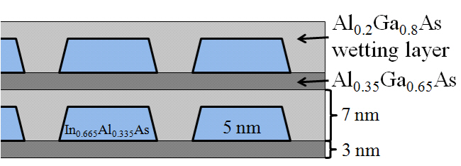
In our simulations, we used the structure described by Table 1 which used the layered quantum dot structure shown in Fig. 1. The composition of the waveguide layers are linearly graded from x = 0.35 to x = 0.65. For comparison purposes, we used Al0.35Ga0.65As waveguides when we simulated the equivalent separate confinement hetero structure (SCH). The SCH configuration has a V number of 9.46 at 808 nm wavelength, meaning that 18 modes can exist in the waveguide as a result of the large optical cavity. This also means that the GRIN-SCH configuration will have multiple modes as well. The active region (shown in Fig. 1) contained multiple layers of quantum dots where each layer contained a 1.0x10¹¹ dots/cm2 dot distribution.The dot composition (x=0.665) and size (10 nm diameter,5 nm height) was selected so that the gain peaked near 808 nm. When multiple quantum dot layers were used, each layer was separated by 3 nm barrier layers of undoped Al0.35Ga0.65As. The total cavity length was 3 mm with a front and back reflectivity of 2% and 90%, respectively.These last two parameters were selected as they are typical for high power laser diodes.
Our structure was simulated using LASTIP[15], a simulation program created by Crosslight Software Inc. This software operates by using a finite-element method which maps the hole density, electron density and electric potential within a given structure. From these, all other properties of interest can be extrapolated. The electronic properties are found from using Poisson’s equation and the current continuity equations, while the optical properties are calculated from the wave equation and the photon rate equation. The electronic and optical properties are connected by the stimulated emission rate equation.
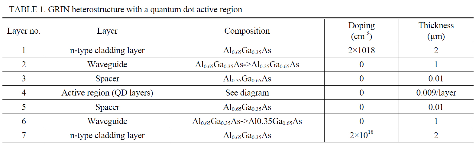
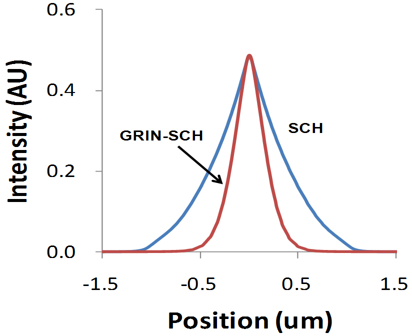
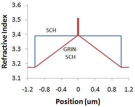
Figures 2 and 3 show the lateral profile of the refractive index and wave intensity, respectively, of a SCH laser and a GRIN-SCH laser with the same 2 ㎛ waveguide width using 6 layers of quantum dots. We chose 6 layers arbitrarily as the intensity profile did not change did not depend on layer number. As expected, this follows the trend seen in quantum well lasers where the fundamental lateral mode is prominent for large (~㎛) graded waveguides while the appearance of higher order modes reduces the optical confinement in the SCH structures, as shown in Fig. 4.Figure 4 also shows that the difference in confinement factors increases with the waveguide size. These two points support the idea that with quantum dots, the GRIN-SCH allows for larger optical cavities and therefore, larger output powers.
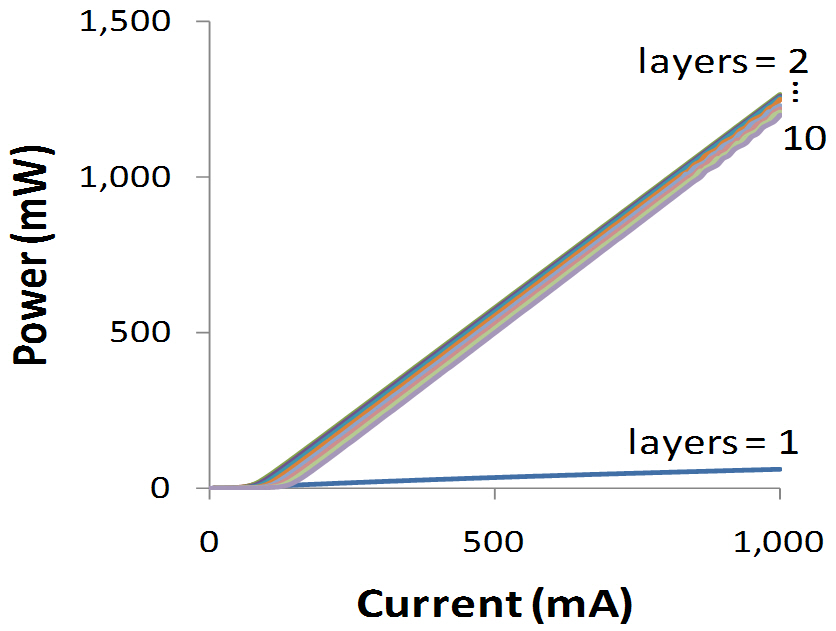
We also simulated our structure using 1 to 10 quantum dot layers to determine the effect of the layer number on
the lasing characteristics. The output power versus injection current (P-I) curves are shown in Fig. 5. With one quantum dot layer, the slope efficiency is low, as expected. As layers are added, the slope efficiency increases to a plateau while, at the same time, the threshold current reaches a minimum value. The further addition of layers results in a steady increase in threshold current while the slope efficiency remains approximately the same.
The plateau in slope efficiency can be seen as the maximum stimulated emission efficiency for the injected carrier. At this maximum efficiency, the addition of more quantum dots (by the addition of layers or higher dot density) does not result in higher optical output power and can be deemed as superfluous. Therefore, with 1.0*1011dots/cm2 dot density,two quantum dot layers may be the optimum arrangement as this produces the maximum slope efficiency for this structure. We note that this will not be the case in other
laser structures as the output power is affected by many other variables such as the mirror reflectivity, internal loss and cavity length. For different structures, our simulations show a similar trend in layer dependence where two layers is not always the optimum case. Further studies should be performed to determine the roles of additional variables.
We used LASTIP to simulate the performance of quantum dots as the active layer in a GRIN-SCH laser diode. Our results showed that properties of higher confinement and maintenance of the Gaussian beam inherited by the GRIN structure still apply when quantum dots are used. In our given structure, we explored the output dependence on the number of quantum dot layers and found that two layers produced the most output power.