검색 전체 메뉴
PDF
맨 위로
OA 학술지
Analysis of a Triangular-shaped Plasmonic Metal-Insulator-Metal Bragg Grating Waveguide
  • 비영리 CC BY-NC
  • 비영리 CC BY-NC
ABSTRACT
Analysis of a Triangular-shaped Plasmonic Metal-Insulator-Metal Bragg Grating Waveguide
KEYWORD
Plasmonics , Triangular-shaped MIM Bragg grating , Bragg reflector , Band-gap , (050.0050) Diffraction and gratings , (240.6680) Surface plasmons , (230.0230) Optical devices , (050.2770) Gratings
  • I. INTRODUCTION

    During the past few decades, due to the diffraction limit of light [1], design, implementation, and application of subwavelength photonic devices, such as waveguides, couplers etc. have faced basic problems and difficulties. In recent years, researchers in the field of plasmonics, investigating the properties and applications of the surface plasmon polaritons (SPP) and localized plasmons [2-4], have introduced a new class of highly miniaturized optical devices to the world [5, 6]. These days SPPs have an important role in the fabri-cation of devices, with a greater confinement of light at nano-scales without limitations due to lightwave diffraction [7].

    Surface plasmon polaritons are the coupling of the electro-magnetic fields to coherent charge oscillations of conduction electrons [8, 9], at the interface of the metallic and dielectric materials, that are excited in visible and near infrared wave-lengths. Exciting the SPPs, part of the light energy is trans-ferred to the surface plasmons, so that the reflected wave has lower energy compared to the incident light.

    From the application point of view, some novel photonic devices based on SPPs, such as waveguides, directional couplers, reflectors, absorption switches and generalized sensors have been proposed in recent years[ 10-16].

    Two specific kinds of multilayer plasmonic structures are insulator-metal-insulator (IMI) and metal-insulator-metal (MIM) [8], but the MIM heterostructures are appropriate geometries in order to obtain better light confinement. The propagation loss of the MIM structures is higher than that of the IMI ones, but in the nanoscale devices it is negligible [17, 18].

    Among the band-gap structures, some kinds of plasmonic Bragg reflectors have recently been introduced. A low-loss index-modulated (In-M) Bragg reflector was investigated by Hosseini et al. [14]. A thickness-modulated (Th-M) [19] and one with both thickness and index modulated profile [13] have been proposed in order to achieve a wider band-gap. Most recently Shibayama et al. have introduced an apodized Th-M Bragg reflector [20] to reduce the side lobes of the transmission spectrum. Liu et al. have introduced a sawtooth profile Bragg reflector [21] which has a narrower band-gap and slightly reduced rippling in the transmission spectrum, compared to the step Bragg reflector. But the main problem with such a profile is that we cannot directly apply the Bragg condition to the structure in order to calculate the lengths of the different layers because the sawtooth profile is repeated completely through the structure and its length equals the sum of lengths of different parts in conventional Bragg structures.

    In this paper, we have introduced two new thickness-modulated (Th-M) and index-thickness-modulated (In-Th-M) triangular-shaped grating MIM Bragg reflectors, whose band-gaps are narrower than those of the same Th-M and In-Th-M step-type structures respectively, and wider than those of the similar sawtooth profile structures. In comparison between the sawtooth and triangular-shaped structures, it is revealed that a smoother transmission spectrum could be achieved by the sawtooth profile. Thus, in order to com-pensate the smaller reduction of rippling, the apodization operation is performed on the new triangular Bragg gratings and a smoother transmission spectrum could be achieved compared to the conventional Bragg reflectors.

    II. ANALYSIS METHOD

    The dispersion relation of a simple MIM waveguide with the assumption of infinite structure and the form of exp[i(β x?ω t)] for the field components propagating in the x-direction for the fundamental TM mode, with Ex, Ey and Hz field components, is given by the following equations [8, 22]

    image

    where k0 is the free space wave-number and ε d, εm, and t are the dielectric constants of dielectric and metal and the dielectric thickness, respectively, as shown in FIG. 1. The effective refractive index of the waveguide can be determined by:

    image

    In this paper, the propagation of SPPs in these structures is simulated, using a two-dimensional FDTD method, accomplished with an auxiliary differential equation (ADE) approach[23]. All the software has been prepared in C++ and Matlab language and environment. The absorbing boundary conditions for all the boundaries of the computational window are convolutional perfectly matched layer (CPML) with the absorption

    loss of about -90 dB [24]. The grid sizes in x and y directions are Δ x= Δ y =4 nm, and considering the Courant limit, the time step is

    image

    where c is the speed of light in free space. A modulated Gaussian point source is located at the middle of the feeding waveguide.The number of time steps in our simulation is 60000.

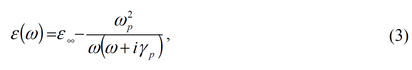
    In our simulations, the metallic cladding layers are assumed to be silver, characterized by the Drude dispersion model[25]:

    image

    where the material-dependant constants ω p and γ p are the bulk plasma and damping frequency, respectively. ε is the dielectric constant at the infinite frequency and the parameters of the Drude model are chosen to be ε=3.7, γ p=2.73×10¹³ Hz and ω p= 1.38×10¹⁶ Hz at λ=1550 nm [25].

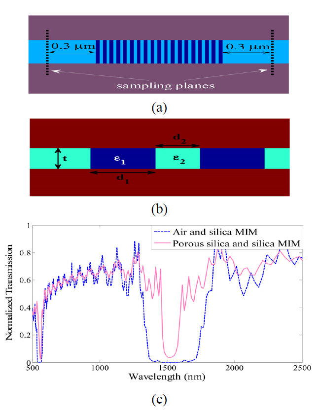
    The input and output sampling planes are displayed in FIG. 2.(a), and the number of periods for all the structures is N=19. The normalized transmission can be defined as │Hy,out(λ )/Hy,in(λ)│, where Hy,out(λ) and Hy,in(λ) are the Fourier transform of the Hy component at the output and

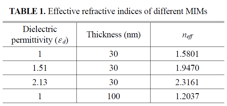
    [TABLE 1.] Effective refractive indices of different MIMs

    label

    Effective refractive indices of different MIMs

    input planes, respectively.

    Solving the dispersion relation equations (1-2) in mathematical software, we obtain the effective refractive indices of MIM structures with various dielectrics and insulator widths as given in TABLE 1.

    According to the Bragg condition d1Re{neff ,1}+d2Re{neff ,2}=nλb/2 where λb is the Bragg wavelength, which is assumed to be 1550 nm here, the thicknesses are chosen as d1 and d2 in order to realize the Bragg condition.

    III. RESULTS AND DISCUSSIONS

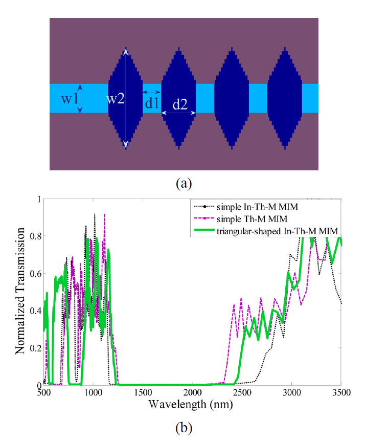
    Two different In-M MIM Bragg gratings, with different insulators, illustrated in FIG. 2 have been simulated. In the first one air and silica with ε d=2.13, and in the second structure porous silica with ε d=1.51 and silica have been chosen as the insulators. As depicted in FIG. 2. (c), the band-gap of the second Bragg grating is narrower than that of the first one, due to the lower contrast of the effective refractive indices.

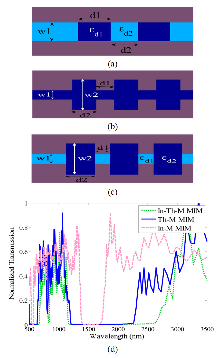
    FIG. 3 represents the In-M, Th-M, and In-Th-M MIM structures, which have been analyzed in [13, 14] and [19],respectively by a transfer matrix method. For the Bragg reflector shown in FIG. 3. (a), the dielectric width is w1=30 nm,ε d1=2.13 (SiO2) and ε d2=1 (air), the effective indices are Re{neff,1}=2.3, and Re{neff,2}=1.5 and their corresponding lengths are d1=168 nm and d2=244 nm. In FIG. 3. (b),the widths of dielectric slits for two alternating stacked MIM waveguides are w1=30 nm and w2=100 nm, which are filled with air, and their corresponding lengths are d1=244 nm and d2=324 nm. In FIG. 3. (c), the slit widths are w1=30 nm and w2=100 nm which are filled with SiO2 and air, respectively and d1=168 nm and d2=324 nm.

    Considering the approximated formula for calculating the band-gap width of a 1D photonic crystal [26], and also the equations (1) and (2), for a structure that consists of two alternately stacked MIM waveguides, the parameters that affect the neff and thereupon Δλg, the band-gap width,are mostly permittivity and thickness of the dielectric region. Here we have shown that with different configurations made by changing these principle factors different widths of band-gaps can be obtained.

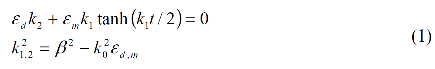
    As demonstrated in FIG. 3. (d), the band-gap of a Th-M Bragg reflector compared to that of the In-M one, and also

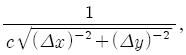
    the band-gap of an In-Th-M structure compared to that of the Th-M one are wider. In the In-Th-M structure because of utilizing different dielectrics and thicknesses in these MIM waveguides, the contrast between two effective refractive indices of MIM waveguides increases and a wider band-gap is expected.

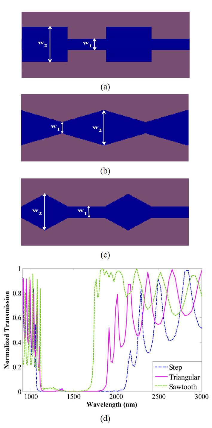
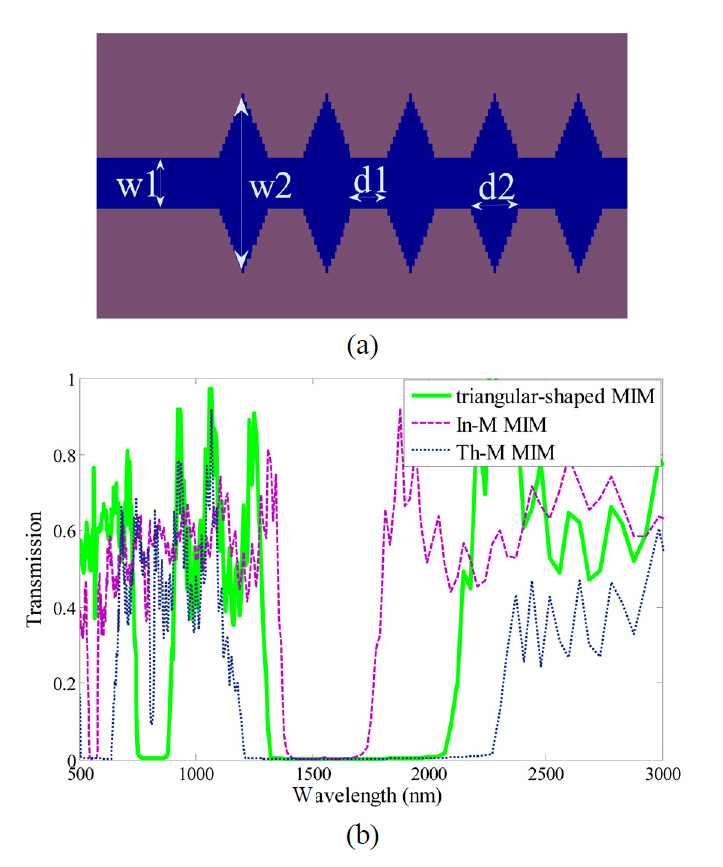
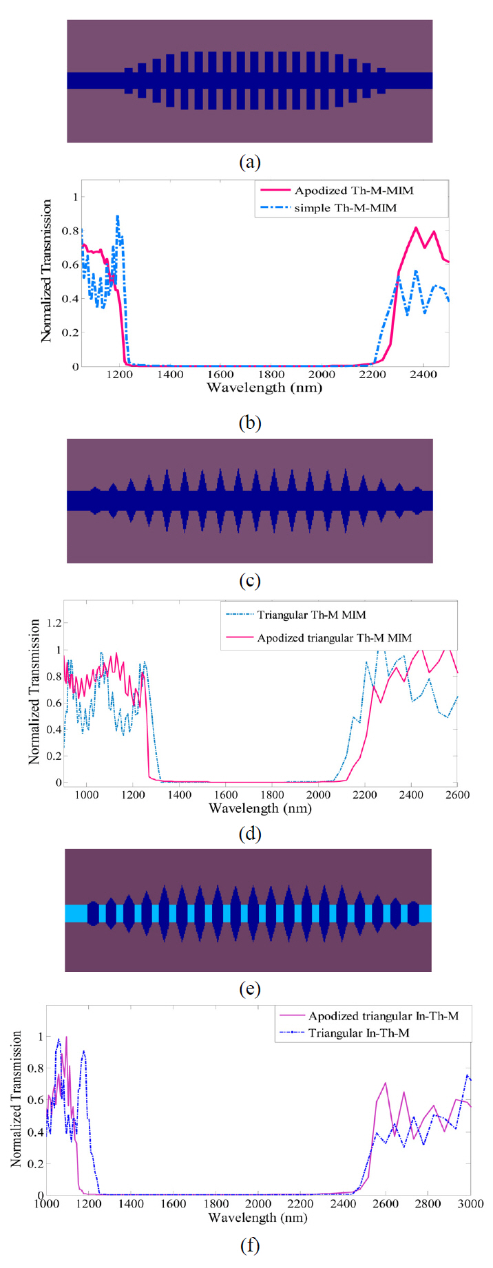
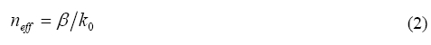
    A new triangular-shaped Bragg grating structure shown in FIG. 4. (a), is proposed here. This proposed structure,compared to a simple Th-M MIM with the same w1, w2,d1, and d2, has a narrower band-gap. If we define an effective insulator width as weff=As/d2 in the MIM structures,where As is the area of the corrugated part, for triangularshaped grating waveguides this parameter is smaller than that of a simple Th-M structure. Due to Eqs. (1) and (2),and also according to the parameter values of TABLE 1,the structures with smaller insulator width, have larger neff.

    So, the contrast between the effective refractive indices of the triangular-shaped grating waveguide parts is less than that of a simple Th-M structure, and a narrower photonic band-gap is expected from the triangular-shaped one, as shown in FIG. 4. (b).

    With the same reasoning, the band-gap of a triangularshaped grating In-Th-M MIM will be narrower than that of the In-M MIM and wider than that of the Th-M MIM,as illustrated in FIG. 5. (b).

    Liu et al. have introduced a kind of grating with sawtooth profile which has a narrower band-gap than a similar conventional step Bragg reflector [21]. Moreover they have claimed that with the sawtooth profile the ripples in the pass-band of the transmission spectrum would be reduced. We have simulated similar structures of conventional step shape, sawtooth and triangular shaped Bragg grating profiles and compared the results. FIG. 6 represents the transmission spectra of these three different gratings simulated in the same conditions.The band-gap width of the triangular-shaped structure (800 nm) is 26% narrower than that of the step one and 23%wider than that of the sawtooth-shaped one. The principle parameters of the Bragg structures, such as the widths and the lengths of the layers in both the sawtooth and triangularshaped reflectors are the same as those of the step structure,but according to different shapes, the band-gaps with different widths are expected.

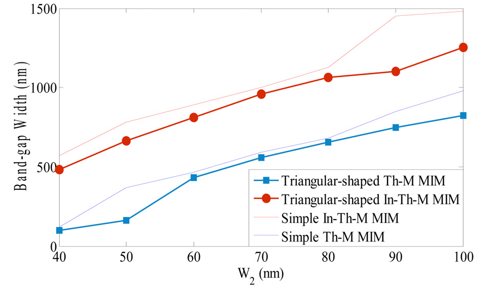
    With smaller w2 the band-gaps become narrower. The variation of the band-gap width versus w2 is depicted in

    FIG. 7, in which the band-gap is defined as the band where the transmission coefficient becomes under -30dB [20]. In FIG. 7, as w2 increases, the band-gap becomes wider, but as illustrated in FIG. 7 for all values of parameter w2, in both of the triangular-shaped structures the band-gaps are narrower than the similar simple gratings.

    In addition, the depths of the ripples in the triangular and sawtooth shaped reflectors are respectively (18%) and (50%)less than that of the conventional step one. In order to compensate this smaller reduction of the ripples in our proposed structure compared to the sawtooth-shaped reflector, we have utilized the apodization operation.

    Shibayama et al. have investigated the effect of apodization on a simple Th-M step structure [20] and have shown that with this operation on the 5 or 9 periods of the grating at both input and output ports, the side lobes in the transmission spectrum are well suppressed [27]. Again, to verify our code, we have first simulated the same structure as that of [20] as depicted in FIG. 8. (a). The same results have been obtained, as shown in FIG. 8. (b).

    Now we show that if a similar procedure is performed on the triangular-shaped grating MIMs, the resultant band-gaps would approximately remain as wide as those of the simple gratings, but the side lobes would be noticeably reduced.FIG. 8 illustrates the apodized triangular-shaped grating,Th-M and In-Th-M gratings and also their transmission

    IV. CONCLUSION

    In this paper, we have proposed a new triangular-shaped MIM Bragg grating structure, whose band-gap is narrower than that of the simple step and wider than that of the sawtooth-shaped Bragg grating. Also, an apodization procedure has been carried out on these new MIM waveguides, in order to cause the side lobes of the transmission coefficient to be considerably suppressed compared to the conventional simple step Bragg reflectors.

참고문헌
  • 1. Liu Z, Lee H, Xiong Y, Sun C, Zhang X 2007 Far-field optical hyperlens magnifying sub-diffraction-limited objects [Science] Vol.315 P.1686 google cross ref
  • 2. Rather H 1988 Surface Plasmon google
  • 3. Sugawara Y, Kelf T. A, Baumberg J. J 2006 Strong coupling between localized plasmons and organic excitonsin metal nanovoids [Phys. Rev. Lett.] Vol.97 P.266808 google cross ref
  • 4. Kong F. M, Huang H, Wu B. I, Kong J. A 2008 Analysis of the surface magnetoplasmon modes in the semiconducor slit waveguide at terahertz frequencies [Progress In Electromagnetics Research PIER] Vol.82 P.257-270 google
  • 5. Maier S. A 2006 Plasmonics: metal nanostructures for subwavelength photonic devices [IEEE J. Select. Topics Quantum Electron.] Vol.12 P.1214-1220 google cross ref
  • 6. Liaw J. W, Kuo M. K, Liao C. N 2005 Plasmon resonances of spherical and ellipsoidal nanoparticles [J. Electromagn.Waves and Appl.] Vol.19 P.1787-1794 google cross ref
  • 7. Wu J. J, Yang T. J, Shen L. F 2009 Subwavelength microwave guiding by a periodically corrugated metal wire [J. Electromagn. Waves and Appl.] Vol.23 P.11-19 google cross ref
  • 8. Maier S. A 2007 Plasmonics: Fundamentals and Applications google
  • 9. Lin L, Blaikie R. J, Reeves R. J 2005 Surface-plasmonenhanced optical transmission through planar metal films [J. Electromagn. Waves and Appl.] Vol.1 P.634-637 google
  • 10. Zhang Q, Hung X. G, Lin X. S, Tao J, Jin X. P 2009 A subwavelength coupler-type MIM optical filter [Opt. Express] Vol.17 P.7549-7554 google cross ref
  • 11. Min C, Veronis G 2009 Absorption switches in metaldielectric-metal plasmonic waveguides [Opt. Express] Vol.17 P.10757-10766 google cross ref
  • 12. Park J, Kim H, Lee B 2008 High order plasmonic Bragg reflection in the metal-insulator-metal waveguide Bragg grating [Opt. Express] Vol.16 P.413-425 google cross ref
  • 13. Liu J. Q, Wang L. L, He M. D, Huang W. Q, Wang D, Zou B. S, Wen S 2008 A wide bandgap plasmonic Bragg reflector [Opt. Express] Vol.16 P.4888-4894 google cross ref
  • 14. Hosseini A, Massoud Y 2006 A low-loss metal-insulatormetal plasmonic Bragg reflector [Opt. Express] Vol.14 P.11318-11323 google cross ref
  • 15. Lezec H. J, Degiron A, Devaux E, Linke R. A, Martin-Moreno L, Garcia-Vidal F. J, Ebbesen T. W 2002 Beaming light from a subwavelength aperture [Science] Vol.297 P.820-822 google cross ref
  • 16. Kim S. A, Kim S. J, Lee S. H, Park T. H, Byun K. M, Kim S. G, Shuler M. L 2009 Detection of avian influenza-DNA hybridization using wavelength-scanning surface plasmon resonance biosensor [J. Opt. Soc. Korea] Vol.13 P.392-397 google cross ref
  • 17. Han Z, Liu L, Forsberg E 2006 Ultra-compact directional couplers and Mach-Zehnder interferometers employing surface plasmon polaritons [Opt. Comm.] Vol.259 P.690-695 google cross ref
  • 18. Zia R, Selker M. D, Catrysse P. B, Brongrsma M. L 2004 Geometries and materials for subwavelength surface plasmon modes [J. Opt. Soc. Am. A] Vol.21 P.2442-2446 google cross ref
  • 19. Hosseini A, Nejati H, Massoud Y “Subwavelength three-dimensional Bragg filtering in integrated slot plasmonic waveguides” P.502-505 google
  • 20. Shibayama J, Nomura A, Ando R, Yamauchi J, Nakano H 2010 A frequency-dependent LOD-FDTD method and its application to the analyses of plasmonic waveguide devices [IEEE J. Select. Topics Quantum Electron.] Vol.46 P.40-49 google cross ref
  • 21. Liu Y, Liu Y, Kim J 2010 Characteristics of plasmonic Bragg reflectors with insulator width modulated in sawtooth profiles [Opt. Express] Vol.18 P.11589-11598 google cross ref
  • 22. Jeong I. S, Park H. R, Lee S. W, Lee M. H 2009 Polymeric waveguides with Bragg gratings in the middle of the core layer [J. Opt. Soc. Korea] Vol.13 P.294-298 google cross ref
  • 23. Taflove A, Hagness S. C 2000 Computational Electrodynamics. The Finite-difference Time-domain Method google
  • 24. Zhang Y. Q, Ge D. B 2009 A unified FDTD approach for electromagnetic analysis of dispersive objects [Progress InElectromagnetics Research PIER] Vol.96 P.155-172 google
  • 25. Hosseini A, Nejati H, Massoud Y 2008 Modeling and design methodology for metal-insulator-metal plasmonic Bragg reflectors [Opt. Express] Vol.16 P.1475-1480 google cross ref
  • 26. Yeh P 1988 Optical Waves in Layered Media google
  • 27. Sun N. H, Liau J. J, Kiang Y. W, Lin S. C, Ro R. Y, Chiang J. S, Chang H. W 2009 Numerical analysis of apodized fiber Bragg gratings using coupled mode theory [Progress In Electromagnetics Research PIER] Vol.99 P.289-306 google
이미지 / 테이블
  • [ FIG. 1. ]  A simple MIM waveguide with dielectric thickness of t.
    A simple MIM waveguide with dielectric thickness of t.
  • [ FIG. 2. ]  (a) The whole structure of a step In-M MIM displaying the input and output sampling planes locations, (b) In-M Bragg grating waveguide for two different set of insulators, first: air and silica with d1=245 nm , d2=167 nm , and second: porous silica and silica with d1=169 nm , d2=167 nm, and t=30 nm, and (c) comparison of transmission spectra of these two structures.
    (a) The whole structure of a step In-M MIM displaying the input and output sampling planes locations, (b) In-M Bragg grating waveguide for two different set of insulators, first: air and silica with d1=245 nm , d2=167 nm , and second: porous silica and silica with d1=169 nm , d2=167 nm, and  t=30 nm, and (c) comparison of transmission spectra of these two structures.
  • [ TABLE 1. ]  Effective refractive indices of different MIMs
    Effective refractive indices of different MIMs
  • [ FIG. 3. ]  Three different MIM structures (a) a part of an In-MMIM with w1=30 nm, ε d1=1 (air), and ε d2=2.13 (SiO2), (b) apart of a Th-M MIM with w1=30 nm and w2=100 nm whichare filled with air, (c) a part of an In-Th-M MIM with w1=30nm which is filled with SiO2 and w2=100 nm, filled with air,(d) the normalized transmission spectra of b, c and dstructures.
    Three different MIM structures (a) a part of an In-MMIM with w1=30 nm, ε d1=1 (air), and ε d2=2.13 (SiO2), (b) apart of a Th-M MIM with w1=30 nm and w2=100 nm whichare filled with air, (c) a part of an In-Th-M MIM with w1=30nm which is filled with SiO2 and w2=100 nm, filled with air,(d) the normalized transmission spectra of b, c and dstructures.
  • [ FIG. 4. ]  (a) A triangular- shaped Th-M MIM with w1=30 nmand w2=100 nm filled with air and (b) its transmissionspectrum, compared to those of similar In-M and Th-M MIMones.
    (a) A triangular- shaped Th-M MIM with w1=30 nmand w2=100 nm filled with air and (b) its transmissionspectrum, compared to those of similar In-M and Th-M MIMones.
  • [ FIG. 5. ]  (a) A triangular-shaped grating In-Th-M MIM withw1=30 nm filled with SiO2 and w2=100 nm filled with air and(b) the transmission spectrum of the displayed structure,compared to those of Th-M and In-Th-M MIMs. Its band-gapis wider than that of the Th-M and is narrower than that of theIn-Th-M one.
    (a) A triangular-shaped grating In-Th-M MIM withw1=30 nm filled with SiO2 and w2=100 nm filled with air and(b) the transmission spectrum of the displayed structure,compared to those of Th-M and In-Th-M MIMs. Its band-gapis wider than that of the Th-M and is narrower than that of theIn-Th-M one.
  • [ FIG. 6. ]  A (a) step, (b) sawtooth and (c) triangular-shapedBragg reflector. (d) The transmission spectra of these threekinds of Bragg gratings.
    A (a) step, (b) sawtooth and (c) triangular-shapedBragg reflector. (d) The transmission spectra of these threekinds of Bragg gratings.
  • [ FIG. 7. ]  Variation of the band-gap width versus the height ofthe triangle in two new proposed structures.
    Variation of the band-gap width versus the height ofthe triangle in two new proposed structures.
  • [ FIG. 8. ]  Side lobes are well suppressed in apodized structures,(a) an apodized Th-M MIM, (b) comparison of simple andapodized Th-M MIMs transmission spectra, (c) an apodizedtriangular-shaped grating Th-M MIM, (d) comparison of thesimple and apodized triangular-shaped grating Th-M MIMstransmission spectra, (e) an apodized triangular-shaped gratingIn-Th-M MIM, (f) comparison of the simple and apodizedtriangular-shaped grating In-Th-M MIMs transmission spectra.
    Side lobes are well suppressed in apodized structures,(a) an apodized Th-M MIM, (b) comparison of simple andapodized Th-M MIMs transmission spectra, (c) an apodizedtriangular-shaped grating Th-M MIM, (d) comparison of thesimple and apodized triangular-shaped grating Th-M MIMstransmission spectra, (e) an apodized triangular-shaped gratingIn-Th-M MIM, (f) comparison of the simple and apodizedtriangular-shaped grating In-Th-M MIMs transmission spectra.
(우)06579 서울시 서초구 반포대로 201(반포동)
Tel. 02-537-6389 | Fax. 02-590-0571 | 문의 : oak2014@korea.kr
Copyright(c) National Library of Korea. All rights reserved.