We demonstrate a high-spatial-resolution imaging and spectroscopy tool using a solid immersion lens(SIL), a hemispherical lens made of high refractive index glass (n ~2). Photoluminescence (PL) images of single CdSe nanocrystals confirm a numerical aperture enhancement factor of ~2, close to the refractive index of the SIL. In particular, a bare-eye observation of PL signals emitted by single nanocrystals with~10 ㎛-2 densities was possible over an ~30 ㎛ diameter region. In addition, the PL spectra of single CdSe nanocrystals were successfully measured at room temperature. Thus, this SIL microscope ensures a simple but powerful method for nanostructure spectroscopy.
High-spatial-resolution imaging has been demonstrated by reducing or even breaking the diffraction limit, using microscopic techniques, such as confocal laser scanning microscopy(CLSM) [1], near-field scanning optical microscopy (NSOM)[2], and stimulated emission depletion (STED) microscopy[3], among others. Solid immersion lens microscopy is one method used to enhance spatial resolution by “immersing” the sample in a solid material of a certain refractive index(
In general, SILs are in the form of either a hemisphere[5] or a super-hemisphere truncated at
In this paper, we demonstrate a high-spatial-resolution imaging and spectroscopy tool using a hemispherical SIL. We take fluorescence signals from single CdSe nanocrystals as point sources to measure the instrument response. Based on subsequent measurements, our results confirm that the NA enhancement factor is close to the refractive index of the SIL, as expected. In particular, the bare-eye observation of PL signals emitted by single CdSe nanocrystals becomes possible, in which the PL spectra are successfully measured at room temperature.
II. SIL MICROSCOPE AND EXPERIMENTAL SETUP
A SIL microscope was built on an inverted optical microscope (Ti-U, Nikon, Japan). For the SIL, we used a 2-mm-diameter hemisphere made of S-LAH79 glass (Ohara) having a refractive index of 2.00330 at the helium d-line (587.5618 nm). Note that a refractive index of ~2 is one of the highest values of commercially available glass materials. Moreover, its absorption coefficient at 400 nm is as low as 0.693 cm-1, ensuring UV-visible spectroscopic applications.
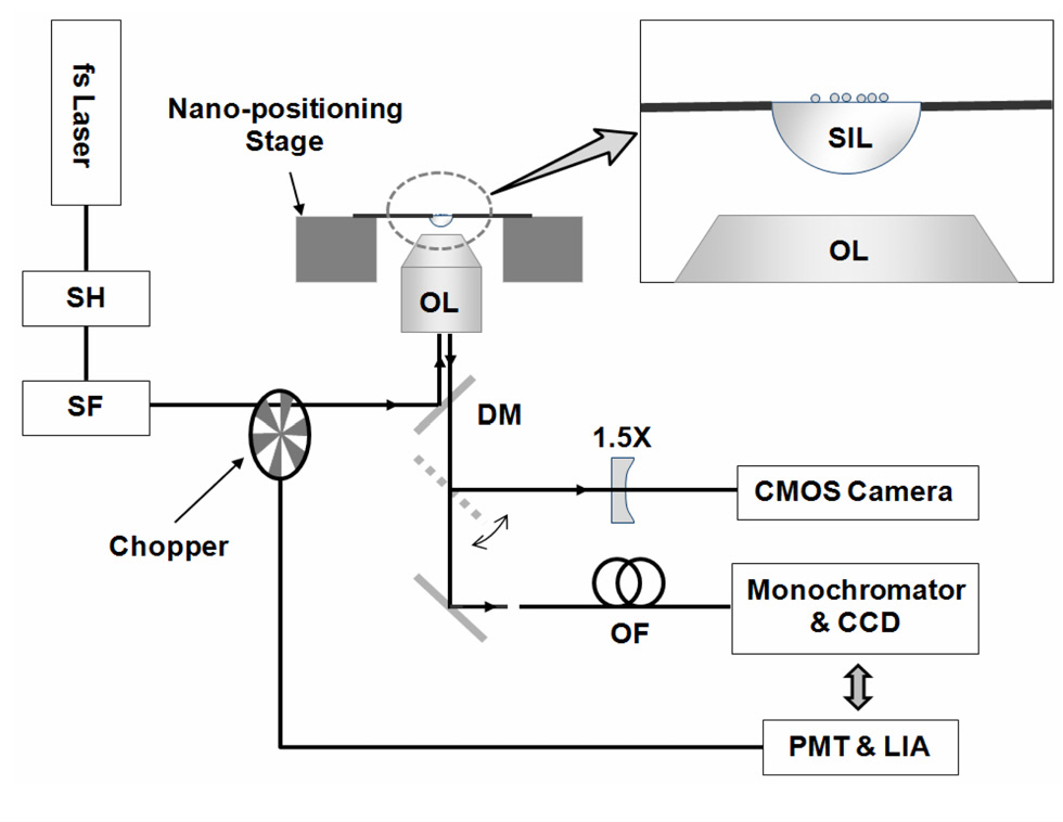
A schematic of the experimental setup is shown in Fig.1. We used a femtosecond Ti:sapphire oscillator system (MaiTai, Spectra Physics, USA) as the light source. The beam was converted to a second harmonic beam (400 nm wavelength) using a β-BaB2O4 (BBO) crystal, and then filtered through a pinhole to make a smooth Gaussian profile. The beam was defocused so that the beam width might be large enough to provide the nearly uniform illumination of the sample plane over a 100 ㎛ spot; we did not measure the actual beam width at the sample plane, but confirmed that the intensity variation was negligible. Subsequently, the beam was guided to the optical microscope, reflected by a dichroic mirror designed for a 400 nm wavelength, and then fed to an objective lens (0.6 NA, 40 × magnification power) before finally reaching the SIL. Then the beam excited the samples on top of the SIL; for the parallel experiments without the SIL, the samples were coated on a glass substrate and placed facing down to the objective lens to minimize aberrations. Fluorescence signals, collected by the same SIL and objective lens, were separated from the laser light using the dichroic mirror, and then guided to the detection ports.
As mentioned above, a SIL microscope offers a high lateral resolution?even in a wide-field detection scheme. For comparison, we built a system that works in both wide-field and scanning modes, modes that can easily be switched by flipping a mirror on the microscope. A complementary metal-oxide semiconductor (CMOS) camera attached at one port was used to take images for a 111㎛ × 89 ㎛ view-field without a SIL, and a 51 ㎛ × 41㎛ view-field with a SIL in wide-field mode. Before taken, the image was further magnified 1.5× to increase the measurement accuracy [7]; the camera was calibrated using a 4-㎛-period calibration grating for both with and without the SIL.
For the pinhole in scanning mode, we used a 633-nm single-mode fiber, in which the core diameter was much smaller than a magnified Airy unit (1.22
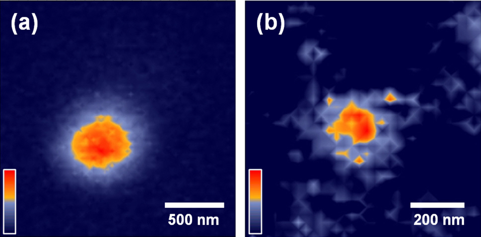
The SIL microscope successfully demonstrated the highspatial-resolution PL imaging of chemically synthesized single CdSe nanocrystals, which were directly coated on the flat surface of the SIL to minimize gap errors (Fig. 2). We could observe the fluorescence intermittency (blinking) effect of single CdSe nanocrystals [8] having ~10 ㎛-2 densities with our bare eyes. Note that this bare-eye observation was possible for diameters of over ~30 ㎛ in aberration-free regions in wide-field mode.
Since the diameter of CdSe nanocrystals (≤ 10 nm) was much smaller than the lateral resolution of the system, the nanocrystals can be assumed to be point sources. Therefore, the intensity pattern of the diffraction-limited spot is the square of the amplitude point spread function(PSF) of the imaging optics, which takes the form of the Airy disc function [9]
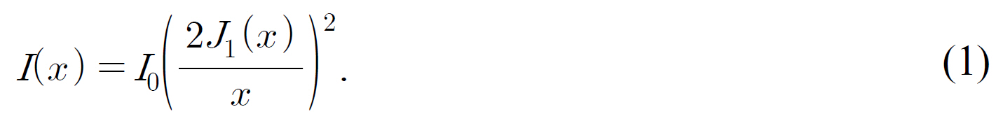
Here,
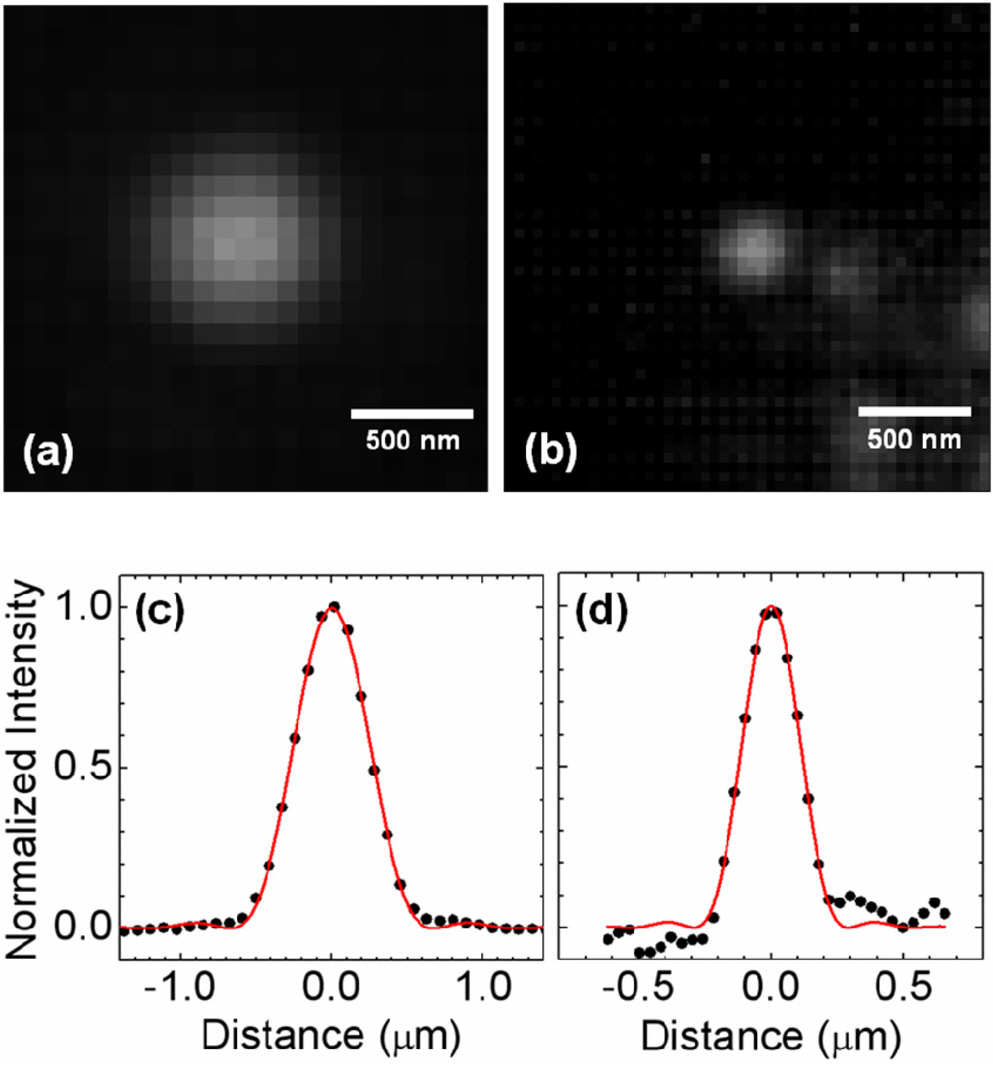
The NA enhancement via SIL imaging becomes more evident when the image is compared to that of a conventional microscope (Fig. 3). The line profiles of the discs, which fit well with the Airy disc function, have a full-width at half-maximum (FWHM) of 245 nm and 565 nm, with and without the SIL, respectively. From the fitting results, the effective NA is 0.54 for the conventional optical microscope,
and 1.22 for the SIL microscope. These values agree well with the single-point resolution,
The PL images of scanning mode exhibit nearly same width as those of wide-field mode (Fig. 4). The fitting results show a FWHM of 569 nm for the scanning optical microscope, and 245 nm for the scanning SIL microscope, due to the fact that we employed extended illumination over the sample plane. Note that if the confocal condition is fulfilled,
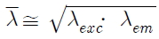
and λexc denotes the excitation wavelength. Calculations then show that an ~150 nm lateral resolution should be realistic for scanning SIL imaging based on the given experimental conditions. In any case, the wide-field SIL microscope provides an affordable NA enhancement factor of 2 while maintaining most merits of a far-field optical microscope.
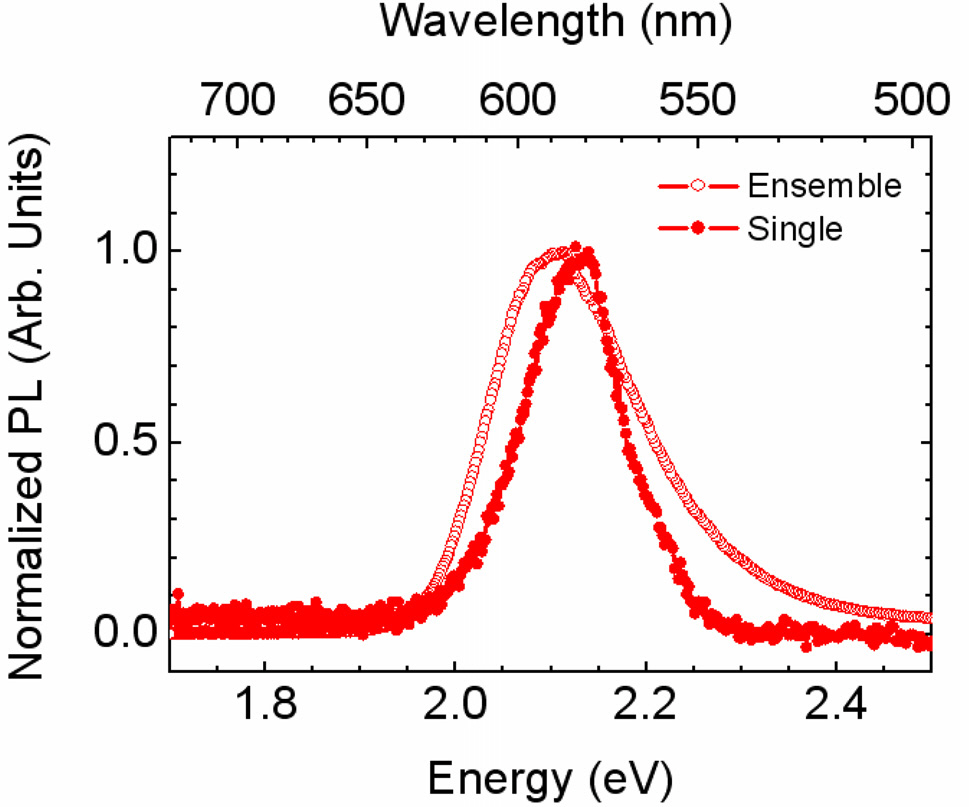
Finally, note that we could measure the spectra of every single point in the PL images. A typical spectrum of a single CdSe nanocrystal at room temperature is shown in Fig. 5. The linewidth of PL signal is 118 meV, which is significantly narrower than that of the inhomogeneously broadened PL spectrum, due to size irregularities in the ensemble state. Subsequently, the SIL microscope offers a simple method for spectroscopy of nanostructures such as multiple quantum wells, quantum dots, nanowires, molecules, organic films, and bio samples.
In summary, we have successfully demonstrated a highspatial-resolution imaging and spectroscopy tool using a hemispherical SIL. Measured PL images of single CdSe nanocrystals confirmed an NA enhancement factor of ~2, close to the refractive index of the SIL. Notably, a bare-eye observation of PL signals emitted by single nanocrystals having ~10 ㎛-2 densities was possible over an ~30 ㎛ diameter region. Furthermore, the PL spectrum from a single CdSe nanocrystal was successfully measured at room temperature using this instrument; thus, the SIL microscope ensures a simple but powerful method for nanostructure spectroscopy.